Quick Links
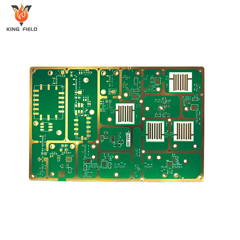
Rigid-flex PCB technology combines the strengths of traditional rigid boards (commonly fabricated with FR-4 or similar materials) and the adaptability of flexible circuits—often built on high-quality polyimide substrates. This hybrid solution enables designers to create complex interconnects, reduce weight, and improve the overall reliability and manufacturability of electronic products, especially in high-density, high-vibration, and space-constrained environments.
|
Feature |
Rigid PCB |
Flex PCB |
Rigid-Flex PCB |
|
Structure |
Only rigid layers (FR-4) |
Only flexible layers (polyimide) |
Combined rigid & flexible sections |
|
Bendability |
None |
Dynamic/static, high bend cycles |
Targeted bends, between rigid zones |
|
Cost |
Lowest |
Mid-Range |
Highest (but most versatile) |
|
Typical Use |
Bulk electronics |
Wearables, connectors, displays |
Aerospace, medical, advanced IoT |
Rigid-flex PCBs are especially advantageous in applications where electronic assemblies must withstand repeated flexing, vibration, shock, or temperature cycling. Common environments include aerospace electronics, medical devices, military-grade equipment, rugged wearables, and the fast-growing world of IoT.
Modern electronics—and especially mission-critical devices—face a challenging blend of demands: miniaturization, weight reduction, resistance to mechanical shock and vibration, and uncompromising reliability. Traditional rigid PCBs alone often cannot meet these standards, particularly in aerospace, medical, military, or rugged consumer products. The rigid-flex PCB emerges as an elegant solution to many such pain points, thanks to its advanced materials, thoughtful stack-up, and unique hybrid construction.
Aerospace, defense, industrial, and medical devices frequently operate under intense mechanical stress: repeated shock, vibration, flexing, rapid temperature swings, and even exposure to harsh chemicals or moisture. In these environments, conventional rigid or cable-based assemblies can suffer from cracked solder joints, connector failures, or intermittent open circuits due to vibration fatigue.
Rigid-flex circuits minimize these risks by:
Weight and space reduction are among the major benefits of adopting rigid-flex board design. In weight-sensitive applications like satellites, implantable medical devices, or wearables, every gram counts. By removing the need for traditional cabling, heavy connectors, and supporting hardware, rigid-flex stack-ups deliver compact, clean, and robust electronic platforms.
List: Reliability and Savings Advantages
The Internet of Things (IoT), wearable fitness devices, next-generation smartwatches, and portable medical monitors all demand electronics that are lightweight, miniaturized, and able to withstand repeated bending. In these scenarios, rigid-flex and flex circuit technologies are seeing explosive adoption.
|
Benefit |
Industry Example |
Problem Solved |
|
High Vibration Tolerance |
Aerospace, Automotive |
Prevents cracked solder joints |
|
Reduced Weight/Space |
Medical Implants, Drones |
Enables miniaturization |
|
Increased Durability |
Wearables, IoT, Medical Sensors |
Outlasts cable/connector fatigue |
|
Fewer Failure Points |
Military, Surveillance Cameras |
Eliminates connectors, jumpers |
|
Assembly/Time Savings |
Consumer Electronics, Test Equip |
Streamlines manufacturing |
The unique construction and material choices of rigid-flex boards, combined with thoughtful stack-up and layout, enable electronic assemblies to withstand the toughest environments and longest service lives—often with substantial reduction in both size and complexity.
The choice to implement rigid-flex PCB technology is often dictated by specific mechanical, electrical, or reliability needs that go beyond what either a pure flex PCB or traditional rigid board design can offer. Knowing when to adopt rigid-flex board design guidelines can make all the difference in meeting performance, manufacturability, and cost goals.
Let’s look at some ideal situations where rigid-flex circuit boards deliver clear advantages:
Example Applications:
Rigid-flex circuit technology is not only about fitting into tight spaces or surviving rough conditions. By removing traditional physical design constraints, engineers can:
It’s important to weigh rigid-flex PCB benefits against upfront and ongoing costs:
One of the defining features of a flex PCB or rigid-flex circuit is its ability to bend and conform to the 3D shapes and movement required by modern electronic designs. However, achieving reliable bending performance demands careful attention to mechanical, material, and layout details. The difference between a design that survives millions of bend cycles and one that fails after a few hundred is often found in understanding and applying core flex PCB bendability rules.
Flex circuits are subject to either static or dynamic bending:
Key Insight: Dynamic flex circuits must be designed much more conservatively, with greater bend radius and more robust material and routing practices, to avoid copper fatigue and trace cracking.
The most crucial parameter for flex reliability is the bend radius—the minimum radius the flex section can be curved without risking mechanical or electrical failure.
General guidelines for minimum bend radius:
|
Layer Count |
Static Flex Bend Radius |
Dynamic Flex Bend Radius |
|
1-2 layers |
≥ 6 × flex thickness |
≥ 100 × flex thickness |
|
3+ layers |
≥ 12 × flex thickness |
≥ 150 × flex thickness |
|
Flex Type |
Thickness (mm) |
Recommended Static Bend Radius (mm) |
Recommended Dynamic Bend Radius (mm) |
|
Single-layer (1oz Cu) |
0.10 |
0.60 |
10 |
|
Double-layer (0.5oz Cu) |
0.15 |
0.90 |
15 |
|
Four-layer (0.5oz Cu/layer) |
0.26 |
3.0 |
39 |
The materials selected for your flex PCB or rigid-flex board directly influence bendability, reliability, longevity, cost, and even manufacturability. Understanding the properties of base materials, adhesives, stiffeners, and finishes is essential for applying the most effective rigid-flex PCB design guidelines and meeting industry standards such as IPC-4202, IPC-4203, and IPC-4204.
|
Feature |
Adhesive-Based Flex |
Adhesive-Less Flex |
|
Process |
Bonded w/ adhesive layer |
Directly laminated, no glue interface |
|
Moisture Resistance |
Lower |
Higher (less water absorption) |
|
Temperature Rating |
~120–150°C (limits reflow cycles) |
Up to 250°C or more (ideal for reflow) |
|
Bend Cycles |
Moderate (static preferred) |
Superior (dynamic/million-cycle approved) |
|
Manufacturing Risk |
Higher delamination risk |
Excellent durability, less delam |
|
Cost |
Lower |
Higher initial cost, but better reliability |
For high-reliability and dynamic flex designs, adhesive-less constructions are now considered the gold standard.
|
Material / Component |
IPC Standard |
Typical Use |
Critical Properties |
|
Polyimide film |
IPC-4202 |
Flex substrate/coverlay |
Dk, Tg, moisture absorption, thermal rating |
|
Rolled annealed copper |
IPC-4562 |
Conductors |
Fatigue life, ductility, thickness |
|
FCCL |
IPC-4204 |
Base laminate |
Adhesion, flexibility, reflow resistance |
|
Bondply/adhesive |
IPC-FC-234 |
Layer bonding |
Temp, moisture, dielectric compatibility |
|
FR-4 stiffener |
IPC-4101 |
Rigid support |
CTE match, mechanical support |
|
Metal stiffener |
N/A |
Heavy-duty support |
Shock/vibration, ground connection |
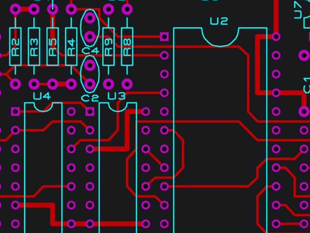
The layout and routing of a flex PCB or rigid-flex circuit is far more than just connecting the dots—it’s where mechanical and electrical engineering truly merge. Proper layout choices are crucial for maximizing bend life, minimizing field failures (such as via cracking or “I-beaming”), and ensuring manufacturability and yield. Below are foundational rules and expert tips to guide you in applying the best rigid-flex PCB design guidelines to your next project.
When using multilayer flex PCBs, more care in routing is needed:
|
Attribute |
Button/Pad-Only Plating |
Panel Plating |
|
Electrical Path |
Only at pads (less copper) |
Copper throughout all traces |
|
Flexibility |
Superior (less overall copper in region) |
Lower (more copper = stiffer) |
|
Solderability |
Higher risk of pad lift-off |
Better for robust assembly |
|
Application |
Dynamic bend, sensitive flex |
Static flex, rigid attachment |
Best Practice: For dynamic, high-flex regions, pad-only (button) plating offers better bend life; for static or rigid-mount regions, panel plating may offer more robust connections.
|
Design Rule / Feature |
Recommended Value / Practice |
|
Trace path in bend zone |
Curved, parallel to bend, no sharp angles |
|
Feature keep-out in bend area |
No pads, holes, vias; observe recommended clearance |
|
Staggered traces (multi-layer) |
Offset between layers, not top-on-bottom alignment |
|
Drill-to-copper distance |
Minimum 8 mil (0.2 mm) |
|
Minimum annular ring (via/pad) |
≥ 8 mil |
|
Use of teardrop pads/vias |
Always in bend and transition regions |
|
Relief holes/cutouts |
Add in wide flex zones for stress reduction |
A well-engineered flex PCB stack-up is the foundation of a reliable rigid-flex board, harmonizing mechanical flexibility with electrical performance. Selecting the right layer count, thickness, and materials helps optimize bendability, signal integrity, EMI shielding, and manufacturability. This section unpacks how to design an effective stack-up aligned with your product’s mechanical and electrical requirements.
Static Flex Stack-Ups: Intended for boards bent once or a few times (e.g., fixed folds inside enclosures). They can tolerate tighter layer counts (up to 8+ layers) and moderate bend radius because the mechanical load is limited after assembly.
Dynamic Flex Stack-Ups: For flex circuits subjected to repeated cyclic bending (hundreds of thousands or millions of cycles), these designs require:
Even-numbered layers with symmetrical arrangements minimize warping and mechanical stress. Properly balanced inner layers help maintain:
Bookbinding Technique: Used in high-layer-count flex PCBs to assemble multiple flex layers by laminating two or more flex circuits back-to-back, separated by bondply. This method enhances mechanical strength without sacrificing flexibility.
Air-Gap Construction: Incorporates controlled air gaps between flex layers or between flex and rigid sections to reduce dielectric constant and loss, improving high-frequency signal transmission and impedance control.
Physical Mock-Ups: Paper or Mylar prototypes help visualize bend zones and mechanical fit before fabrication.
ECAD/MCAD Integration: Use tools like Cadence OrCAD, Altium, or Siemens NX to simulate stack-up zones, bend radii, and mechanical stresses.
Stack-Up Tools: Many PCB manufacturers provide stack-up and material selector tools online, assisting with impedance calculations and material compatibility checks early in the design process.
|
Layer |
Material |
Thickness (mils) |
Copper Weight (oz) |
Notes |
|
1 |
Coverlay (Polyimide) |
1.5 |
N/A |
Protective top layer |
|
2 |
Signal Layer (Cu) |
0.5 |
0.5 oz |
Inner signal traces |
|
3 |
Prepreg (Bondply) |
2.0 |
N/A |
Adhesive dielectric layer |
|
4 |
Signal Layer (Cu) |
0.5 |
0.5 oz |
Inner return/power plane |
|
5 |
Flexible Core (Polyimide) |
1.0 |
N/A |
Flexible backbone |
|
6 |
Signal Layer (Cu) |
0.5 |
0.5 oz |
Bottom layer signal |
|
7 |
Coverlay (Polyimide) |
1.5 |
N/A |
Bottom protective coverlay |
Adhering to industry standards is critical for ensuring that your rigid-flex PCB meets quality, reliability, and manufacturability expectations. IPC standards serve as the backbone for consistent design, fabrication, inspection, and assembly practices across the electronics industry. Below we highlight key IPC standards to guide your rigid-flex PCB project from concept through production.
|
Standard |
Scope |
Relevance |
|
IPC-2221 (Generic Standard on Printed Board Design) |
Covers generic requirements for designing PCBs and other forms of component mounting or interconnecting structures. |
Provides foundational design guidelines applicable to flex, rigid, and rigid-flex PCBs. |
|
IPC-2223 (Sectional Design Standard for Flexible and Rigid-Flex Circuits) |
Defines specialized design rules specifically for flex and rigid-flex circuits, including bend zones, stack-up, and transitions. |
Central for flex PCB bend radius, trace routing guidelines, and keep-out areas. |
|
IPC-6013 (Qualification and Performance of Flexible Printed Boards) |
Specifies manufacturing qualification criteria, acceptance testing, and performance requirements for flexible PCBs. |
Ensures flex and rigid-flex PCBs meet reliability and quality metrics pre-shipment. |
|
IPC-600 (Acceptability of Printed Boards) |
Provides visual and electrical acceptance criteria for completed printed circuit boards, including defect classifications. |
Used for final inspection, defines acceptable flaw limits, including flex-specific concerns. |
|
IPC-A-610 (Acceptability of Electronic Assemblies) |
Defines workmanship criteria for assembled PCBs, including solder joints and component placement quality. |
Critical for rigid-flex PCB assembly, especially at transition zones and connectors. |
|
IPC/EIA J-STD-001 (Requirements for Soldered Electrical and Electronic Assemblies) |
Standard for soldering processes, materials, and acceptability criteria. |
Ensures solder joint reliability for rigid-flex assemblies, including ZIF connectors. |
|
IPC-FC-234 (Guidance for Pressure-Sensitive Adhesives in Flexible Circuits) |
Covers adhesive selection and application instructions specific to PSA materials used in flex circuits. |
Important for reliable bondply and coverlay adhesion in flex and rigid-flex designs. |
Bend Radius and Mechanical Stress Controls: IPC-2223 defines minimum bend radius guidelines based on the number of flex layers and stack-up thickness, critical to preventing conductor fatigue and via cracking.
Transition Zone Design Rules: IPC-2223 and IPC-6013 emphasize keep-out areas around flex-to-rigid transitions—no pads, vias, or traces too close to edges to minimize delamination or fracture.
Laminate and Adhesive Specifications: Choosing IPC-compliant materials ensures performance under extended thermal cycles, bending stresses, and humidity, with IPC-FC-234 guiding adhesive use.
Inspection and Acceptance: Using IPC-600 and IPC-610 criteria allows fabricators and assemblers to classify imperfections appropriately, setting tolerance levels tailored to flex circuit demands.
Assembly Guidelines: Per IPC-A-610 and J-STD-001, assembly in rigid-flex PCBs demands rigorous soldering and moisture control techniques (pre-baking), especially given polyimide’s moisture sensitivity.
IPC standards also prescribe:
|
IPC Standard |
Primary Focus |
Key Benefit |
|
IPC-2221 |
Generic PCB design rules |
Base-level design consistency |
|
IPC-2223 |
Flex/rigid-flex-specific design rules |
Bend zones, transitions, keep-outs |
|
IPC-6013 |
Flex PCB manufacturing qualification and inspection |
Fabrication reliability assurance |
|
IPC-600 |
PCB visual and electrical acceptability |
Defect classification and acceptance limits |
|
IPC-A-610 |
Assembly workmanship |
Assures soldering and component quality |
|
J-STD-001 |
Soldering process |
Consistent and reliable solder joint quality |
|
IPC-FC-234 |
Adhesive handling in flex circuits |
Ensures durable adhesive bonds |
Designing and manufacturing flex PCBs and rigid-flex PCBs involves complex variables that directly influence cost and lead time. Understanding these drivers enables engineers and product managers to optimize designs for faster, more economical production without sacrificing quality or reliability.
|
Cost Factor |
Impact |
Description |
|
Board Size and Shape |
High |
Larger or irregularly shaped flex circuits require more material and complex tooling. |
|
Layer Count |
High |
Each additional layer adds process steps, prepreg, copper, and inspection requirements. |
|
Material Selection |
Medium |
Specialty materials like high-Tg polyimide, no-flow prepregs, and adhesive-less FCCLs cost more. |
|
Copper Thickness and Cross-Hatching |
Medium |
Heavier copper raises cost; cross-hatching saves flexibility, but requires extra process control. |
|
Flex vs. Rigid Sections |
Medium |
Complex rigid-flex stack-ups increase setup and lamination steps. |
|
Drill Hole Size and Count |
Medium |
More holes mean longer drilling time; small holes (<8 mil) add complexity. |
|
Via and Pad Features |
Medium |
Special vias (microvias, blind/buried), large annular rings, and teardrops incur higher costs. |
|
Surface Finishes and Stiffeners |
Medium |
ENIG finishes, stiffener material (Kapton, FR4, metal) and quantity impact cost. |
|
Tolerances and Build Requirements |
High |
Tight electrical/mechanical tolerances require finer manufacturing controls and inspections. |
Inappropriate Bend Requirements Specifying bend radii smaller than fabrication capabilities or IPC guidances creates manufacturing rework and delays.
Incomplete or Ambiguous Design Data Missing key documentation such as flex-to-rigid transition specs, ZIF connector details, stack-up definitions, or drill-to-copper clearances results in engineering back-and-forth and hold-ups.
Design-Related Issues Examples include improper trace routing in bends, via placement errors, or excessive copper planes in flex areas flagged by DFM tools post-submission.
Unclear Assembly Instructions Flex assembly requires pre-bake/moisture control, proper stiffener usage, and fixture guidelines. Missing these details can cause assembler confusion and lost time.
Pro Tip: Providing a complete fabrication drawing and comprehensive specs, coupled with early DFM consultation from your flex PCB manufacturer, dramatically shortens lead times and reduces costly redesigns.
When optimizing cost with turnaround time considerations, remember that:
|
Design Factor |
Cost Impact |
Turnaround Impact |
Mitigation Strategy |
|
Excessive Layer Count |
High |
High |
Limit layers to essential; use bookbinding/air-gap if needed |
|
Small Drill Holes (<8 mil) |
Medium |
High |
Increase drill sizes slightly if performance permits |
|
Complex Via Types (Blind/Buried) |
Medium |
Medium |
Use standard vias where possible |
|
Tight Bend Radius (<IPC standard) |
High |
High |
Design bend radius per IPC-2223 and material specs |
|
Multiple Stack-Up Zones |
Medium |
Medium |
Use ECAD tools to optimize and verify before fab |
|
Adhesive-Less Constructions |
Higher material |
Medium |
Weigh long-term reliability benefits vs upfront cost |
Partnering with the right flex PCB or rigid-flex PCB manufacturer is critical to ensure your sophisticated designs translate into high-quality, reliable products delivered on time. Unlike standard rigid boards, flex and rigid-flex circuits demand specialized fabrication, precise material handling, and stringent quality control to meet demanding electrical and mechanical specifications.
Experience and Production Capability
Materials and Technology
Design for Manufacturability (DFM) Support
Certifications and Quality Assurance
Single-Facility, Turnkey Production
|
Category |
Sample Questions |
|
Experience & Capabilities |
How many years have you produced flex/rigid-flex PCBs? Do you handle high layer count and dynamic flex? |
|
Materials & Technology |
What types of polyimide and FCCL materials do you stock? Do you offer adhesive-less flex? |
|
DFM & Support |
Do you provide DFM reviews and design consultation? What online tools do you offer for quoting and file checks? |
|
Quality Certifications |
Which certifications do you hold (e.g., IPC, ISO, UL)? Share recent audit results? |
|
Assembly & Moisture Control |
What are your pre-bake processes? Can you assemble flex circuits with ZIF connectors reliably? |
|
Lead Time and Scale |
What is your typical quick-turn prototype lead time? Can you scale from 1 prototype to 100,000+ production units? |
Sierra Circuits exemplifies industry best practices, offering:
Designing and manufacturing rigid-flex PCBs is a sophisticated process requiring a holistic approach—from intelligent material selection and stack-up design to precise layout and trusted manufacturing partnerships. Below is a concise summary of key points and best practices drawn from industry standards and field experience to help you succeed with your next high-performance flex circuit.
|
Best Practice |
Why It Matters |
|
Early DFM consultation with manufacturer |
Avoid redesigns, ensure manufacturability |
|
Use IPC-compliant materials and processes |
Meet industry standards for reliability and quality |
|
Maintain proper bend radius and neutral axis design |
Maximize flex circuit lifespan |
|
Prioritize rolled annealed copper for dynamic flex |
Superior copper ductility for repeated bending |
|
Create symmetrical stack-ups |
Reduce mechanical stress and warping |
|
Optimize trace routing and via design |
Prevent mechanical failures and signal issues |
|
Select turnkey manufacturers with flex expertise |
Smooth prototype-to-production transition |
Rigid-flex PCB design blends electrical precision with mechanical necessity—balancing multilayer stack-ups, careful material choices, and elegant routing to create robust solutions for the most demanding industries. With thoughtful application of standards, collaboration with experienced manufacturers, and adherence to proven design rules, your next flex or rigid-flex PCB will excel in durability, performance, and manufacturability.
 Hot News
2026-01-17
2026-01-16
2026-01-15
2026-01-14
2026-01-13
2026-01-12
2026-01-09
2026-01-08