Multilayer PCB
High-quality Multilayer PCBs for medical, industrial, automotive & consumer electronics. Compact design, enhanced signal integrity, and reliable performance—paired with 24h prototyping, fast delivery, DFM support & AOI/ICT testing. Cost-effective, durable, and tailored for high-density, complex applications.
Description
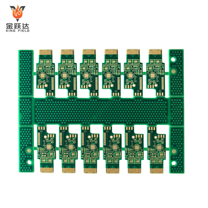
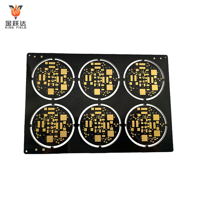
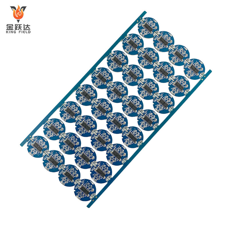
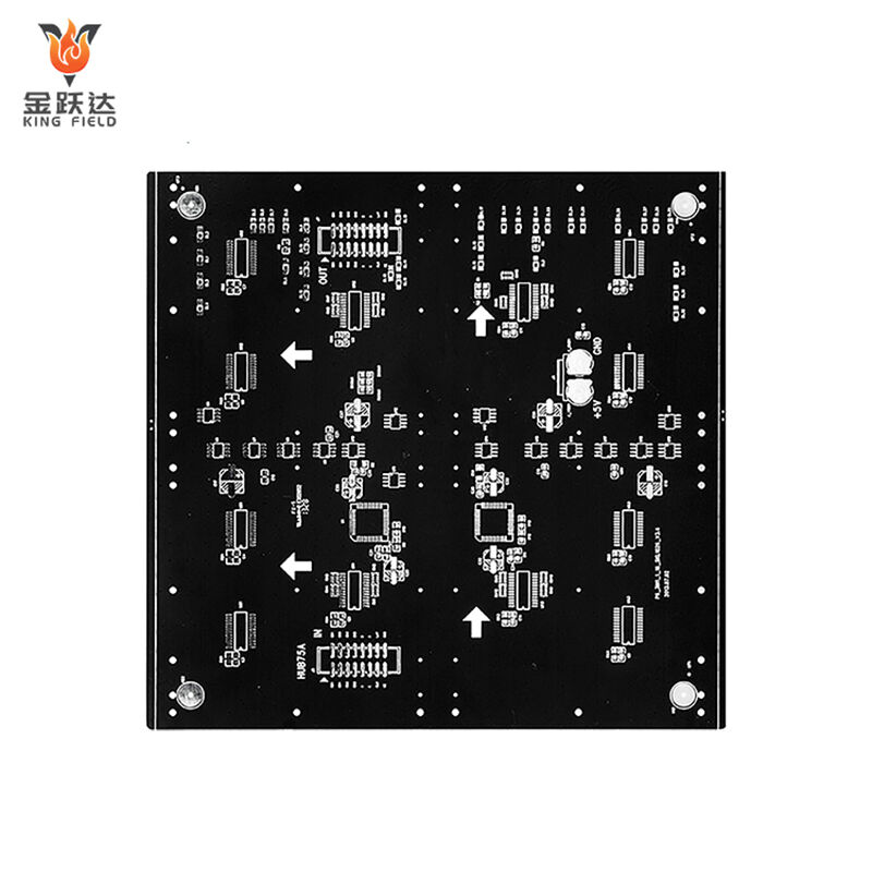
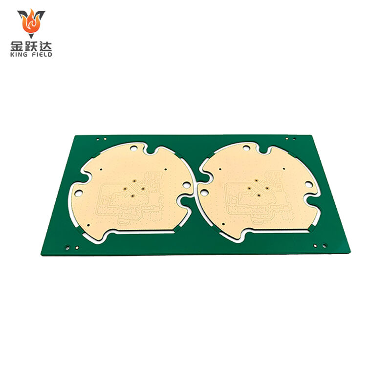
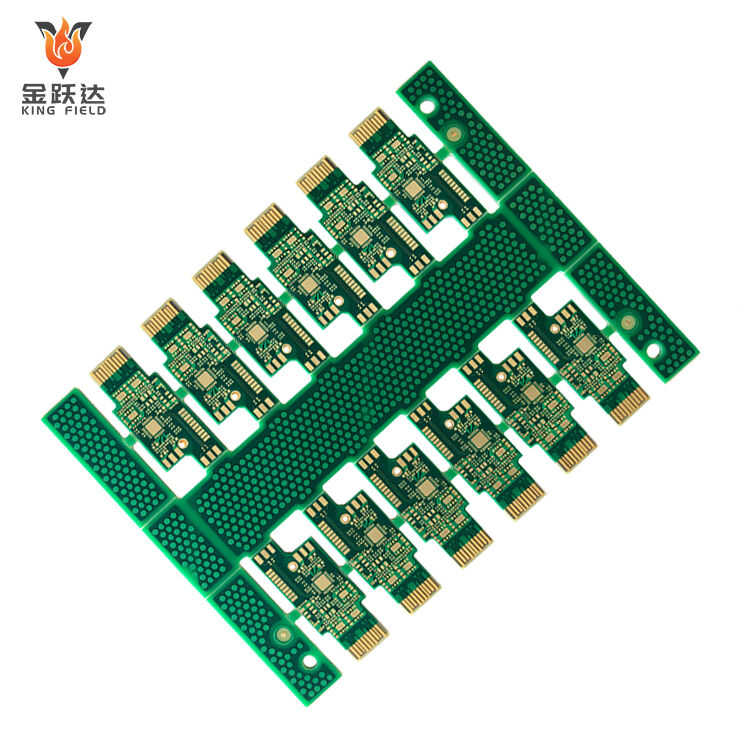
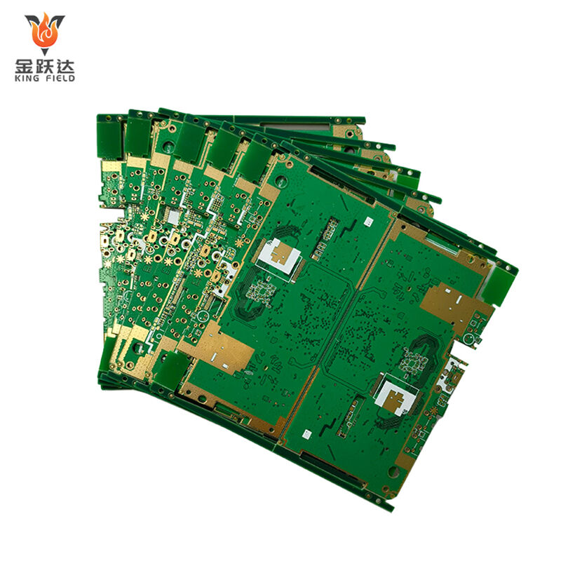
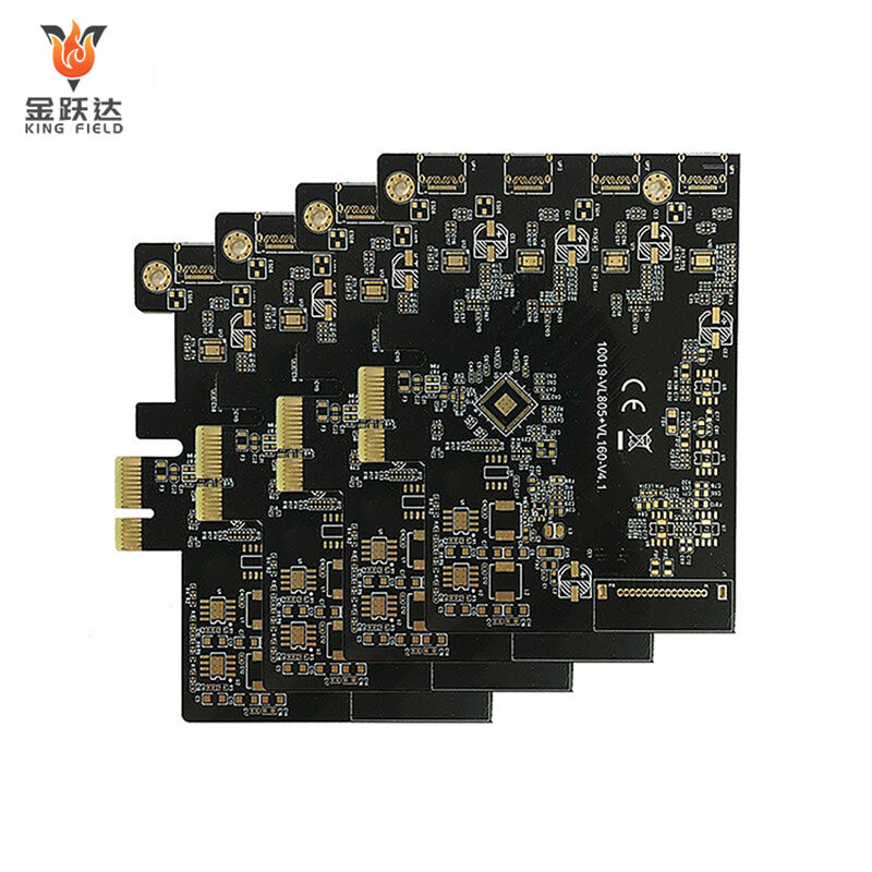
Multilayer PCB Circuit Boards
High-precision, high-density, and high-reliability multilayer printed circuit board solutions.
Multilayer PCBs, or multi-layer printed circuit boards, are circuit boards composed of three or more conductive copper foil layers. Each layer is separated by insulating material, and electrical connections between different layers are achieved through vias formed by drilling and metallization. Compared to single-layer or double-layer PCBs, they offer a more compact layout, higher integration, stronger anti-interference capabilities, and superior circuit performance, meeting the needs of complex electronic devices. However, their manufacturing process is more complex, resulting in higher costs and longer design and manufacturing cycles. These circuit boards are widely used in products with high requirements for circuit complexity, size, and performance, such as smartphones, computers, 5G devices, and automotive electronics. During design and manufacturing, key considerations include layer stack planning, via design optimization, and impedance control to ensure stable operation.
Advantages
Product Advantages
Kingfield multilayer PCBs utilize advanced manufacturing processes and stringent quality control to provide customers with high-performance, high-reliability multilayer printed circuit board solutions.
 |
Advantages of Multilayer PCB Technology A multilayer PCB is a printed circuit board that combines multiple single-layer or double-layer PCBs bonded together with insulating layers and electrically connected between layers via vias. Compared to traditional single-layer or double-layer PCBs, multilayer PCBs offer the following advantages:
|
||||
Product Features
Multi-layer design Supports 1-40 layer PCB design to meet the needs of electronic devices with varying complexity, and can achieve high-density interconnect (HDI) designs with up to 50 layers.
High-precision manufacturing
The minimum line width/spacing can reach 3mil, and the minimum hole diameter can reach 0.2mm, meeting the needs of high-density and high-precision PCB manufacturing.
Customized services
We offer comprehensive customization services, designing and manufacturing multilayer PCB products with different specifications and performance according to customer needs.
High reliability
A rigorous quality control system and 100% electrical testing ensure high product reliability and stability, with an MTBF (Mean Time Between Failures) exceeding 1 million hours.
Excellent thermal stability
Made with high-quality FR-4 substrate, it has excellent thermal stability and mechanical strength, and can work stably in a temperature range of -40℃ to 125℃.
High frequency performance
It supports high-frequency signal transmission and can be used in GHz-level high-speed communication equipment. It has good signal integrity and low insertion loss.
Technical Specifications
|
Technical Specifications Kingfield multilayer PCBs offer superior technical performance, meeting the demands of a wide range of demanding products. |
||||
 |
number of floors | Floors 2-32 | Line width | 3mil |
| Thickness range | 0.4-6.0mm | Line spacing | 3mil | |
| Base material type | FR-4 | Minimum aperture | 0.2mm | |
| Tg value | 130-180℃ | Operating temperature | -40 | |
| Copper foil thickness | 1/2-3oz | Humidity range | 10% | |
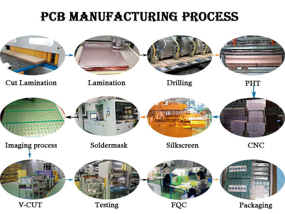
Manufacturing Process
| Kingfield employs advanced multilayer PCB manufacturing processes to ensure product quality and performance. performance. | |||||
|
1. Design and Engineering: |
2. Inner Layer Fabrication: |
3. Lamination: |
4. Drilling: |
||
|
5. Copper plating: |
6. Outer Layer Fabrication: Similar to the inner layer fabrication, circuit patterns are created on the outer copper foil using processes such as photolithography and etching. After the outer layer fabrication is complete, AOI is performed to ensure the accuracy of the circuit patterns. |
7. Solder resist and screen printing:
Solder resist ink is applied to the PCB surface to protect the circuit from external environmental influences. Then, component markings and other information are printed on the PCB surface using a screen printing process. |
8. Testing and Inspection: |
||
Application
Application Scenarios: Kingfield multilayer PCBs are widely used in various electronic devices and industries to meet the needs of different fields.
|
Aerospace: Used in avionics equipment, satellite communication systems, etc., featuring high reliability and radiation resistance. |
Communication equipment: Used in communication equipment such as base stations, routers, switches, and optical modules, supporting high-speed signal transmission and complex circuit designs. |
Medical equipment: Used in medical diagnostic equipment, monitoring equipment, and treatment equipment, characterized by high reliability and stability. |
|
Industrial Control: Applied to industrial automation equipment, PLCs, frequency converters, etc., it features excellent anti-interference capabilities and stability. |
Consumer electronics: Used in consumer electronics products such as smartphones, tablets, and laptops, supporting high-density, miniaturized designs. |
Automotive electronics: Used in automotive electronic control systems, in-vehicle entertainment systems, ADAS, etc., possessing excellent high-temperature resistance and vibration resistance. |
Manufacturing capacity
| PCB Manufacturing Capability | |||||
| ltem | Production capability | Min space for S/M to pad, to SMT | 0.075mm/0.1mm | Homogeneity of Plating Cu | z90% |
| Layer Count | 1~40 | Min space for legend to pad/ to SMT | 0.2mm/0.2mm | Accuracy of pattern to pattern | ±3mil(±0.075mm) |
| Production size(Min & Max) | 250mmx40mm/710mmx250mm | Surface treatment thickness for Ni/Au/Sn/OSP | 1~6um /0.05~0.76um /4~20um/ 1um | Accuracy of pattern to hole | ±4mil (±0.1mm ) |
| Copper thickness of lamination | 1\3 ~ 10z | Min size E- tested pad | 8 X 8mil | Min line width/space | 0.045 /0.045 |
| Product board thickness | 0.036~2.5mm | Min space between tested pads | 8mil | Etching tolerance | +20%0.02mm) |
| Auto-cutting accuracy | 0.1mm | Min dimention tolerance of outline (outside edge to circuit) | ±0.1mm | Cover layer alignment tolerance | ±6mil (±0.1 mm) |
| Drill size(Min/Max/hole sizetolerance) | 0.075mm/6.5mm/±0.025mm | Min dimention tolerance of outline | ±0.1mm | Excessive adhesive tolerancefor pressing C/L | 0.1mm |
| Min percent for CNC slot length and width | ≤0.5% | Min R corner radius of outline(inner filleted corner) | 0.2mm | Alignment tolerance forthermosetting S/M and UV S/M | ±0.3mm |
| maximum aspect Ratio(thickness/hole diameter) | 8:1 | Min space golden finger to outline | 0.075mm | Min S/M bridge | 0.1mm |
Frequently Asked Questions about Multilayer PCBs
Q: What problems arise from an unreasonable multilayer PCB stack-up design? How can they be solved?
A: Signal crosstalk, attenuation, and power instability are likely to occur. Solutions include adhering to the principle of adjacent power and ground layers, isolating sensitive and interfering signal layers, and matching copper foil thickness to ensure power supply.
Q: How to handle common defects in multilayer PCB manufacturing such as lamination misalignment and hole wall plating?
A: Lamination misalignment requires optimizing lamination parameters, using high-precision positioning technology, and selecting a substrate with good thermal stability; hole wall plating defects require improving drilling and pretreatment processes and adjusting plating parameters.
Q: What to do about bridging and cold solder joints during multilayer PCB assembly?
A: Optimize pad size and spacing, control solder paste application, adjust soldering temperature profiles, and clean component leads and pads to remove oxidation contaminants.
Q: How to solve the problem of poor heat dissipation in multilayer PCBs over long-term use?
A: Increase the area of heat-dissipating copper foil, design heat dissipation structures, select high thermal conductivity substrates, distribute heat-generating components, and, if necessary, use embedded tubes or sprayed thermal coatings.
Q: Multilayer PCBs are prone to failure in harsh environments; what countermeasures are available?
A: We employ anti-corrosion surface treatments such as immersion gold coating, apply three-proof coating, optimize equipment sealing design, and select substrate materials suitable for harsh environments.

