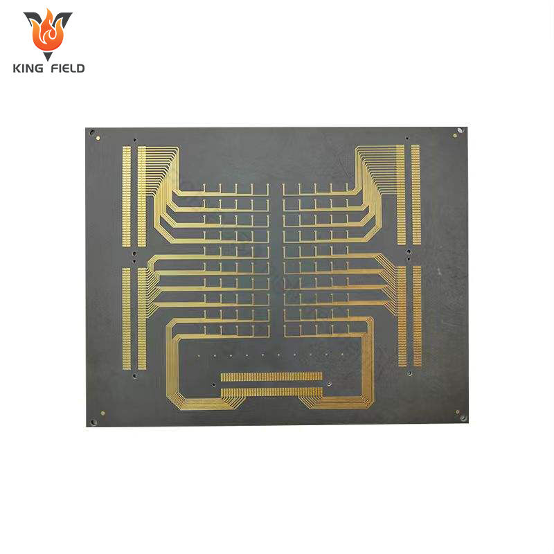
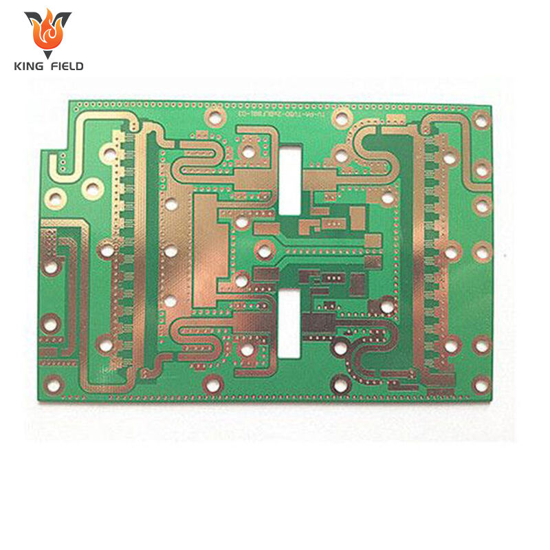
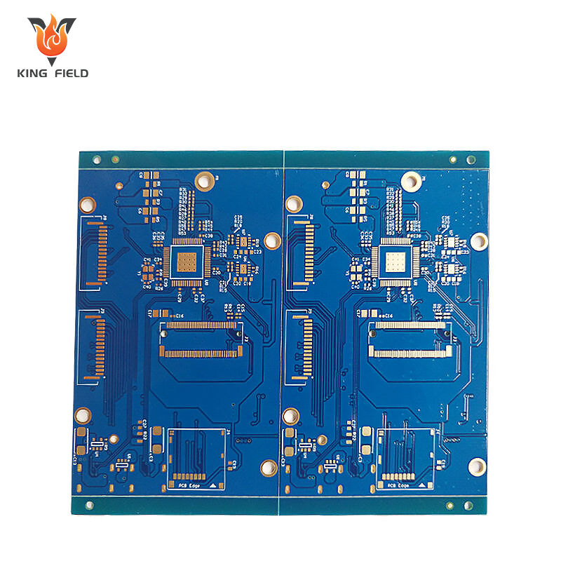
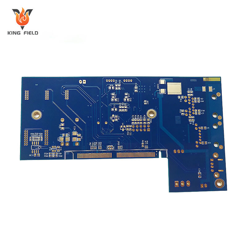
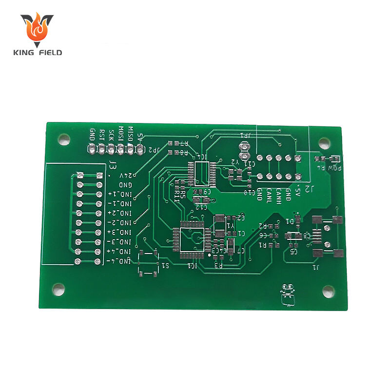
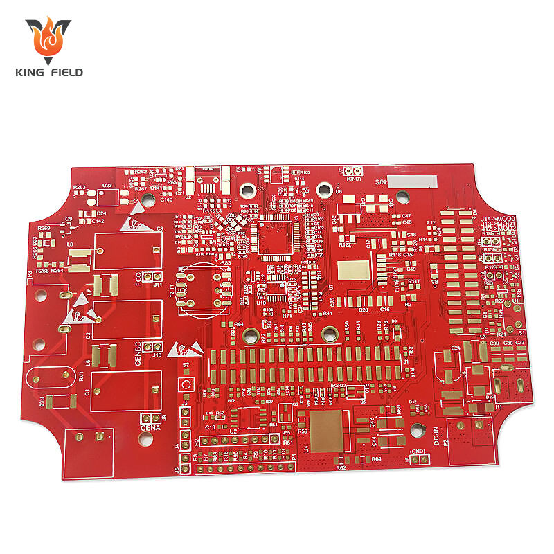
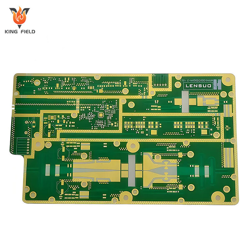
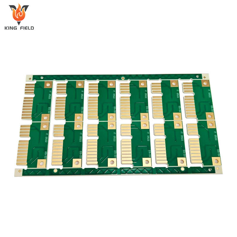
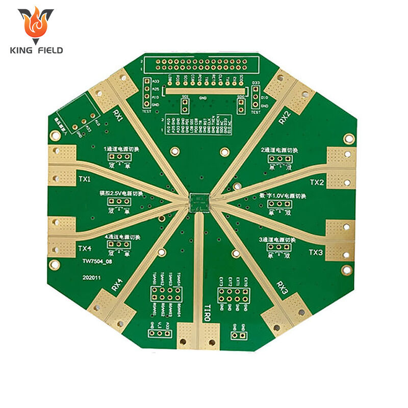
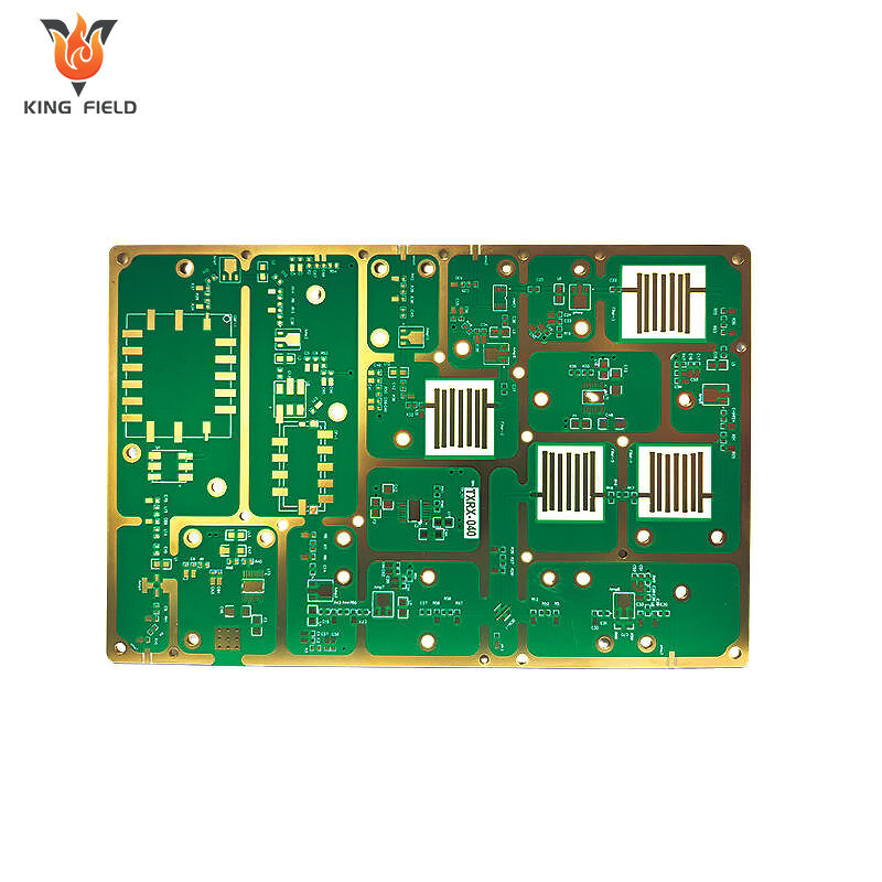
High Frequency PCBs
High-performance High Frequency PCBs for RF, microwave & high-speed signal applications. Premium low-loss materials (PTFE/Rogers), precise impedance control, and 24h prototyping + fast delivery. DFM support & quality testing ensure reliable GHz-frequency performance.
✅ Low-loss materials for signal integrity
✅ Precise impedance control (±5%)
✅ RF/telecom/high-speed data focus
Description
What is a high-frequency PCB?
High frequency PCB is a type of PCB that uses dedicated substrates with low dielectric constant (Dk) and low dielectric loss (Df), such as PTFE and Rogers series. It requires strict impedance control and optimized wiring to reduce parasitic parameters. It is specifically designed for high frequency signal transmission scenarios ranging from 300 MHZ to 3GHz. High-precision printed circuit boards widely compatible with equipment in fields such as communication, military industry, medical care, and consumer electronics.
Characteristics of high-frequency PCBS
The characteristics of high frequency communication circuits are designed around the three core requirements of low loss, high stability, and anti-interference in the transmission of high-frequency signals ranging from 300 MHZ to 3GHz. Each characteristic corresponds to specific material selection, process standards, and application values. The following is a detailed breakdown:
The low-loss characteristic of the substrate
When high-frequency signals are transmitted, energy loss occurs due to the dielectric properties of the substrate. This is the core difference between high frequency circuit and ordinary PCBS.
Key parameters
· Low dielectric constant (Dk) : The dielectric constant determines the signal transmission speed. The lower the Dk value, the faster the signal transmission speed and the smaller the signal delay. The Dk value of high-frequency PCB substrates is usually stable between 2.2 and 4.5 (the Dk of common FR-4 substrates is approximately 4.6 to 4.8), and it is necessary to ensure the stability of Dk under different temperatures and frequencies to avoid signal distortion.
· Low dielectric loss tangent (Df) : The Df value directly reflects the energy loss of the signal in the substrate. The lower the Df, the smaller the loss. The Df value of high-frequency PCB substrates is generally less than 0.002 (the Df of ordinary FR-4 is about 0.02), which can effectively reduce signal attenuation and is especially suitable for long-distance and high-frequency signal transmission.
Typical substrate
· PTFE (Polytetrafluoroethylene) : Dk≈2.1, Df≈0.0009, high-temperature resistance (above 260℃), strong chemical stability, it is the first choice for high-demand scenarios such as military industry and satellite communication.
· Rogers series (such as RO4350B) : Dk≈3.48, Df≈0.0037, with excellent impedance stability, suitable for 5G base stations and RF modules.
· High-frequency epoxy resin board: Lower cost, Dk≈3.5-4.0, meeting the basic requirements of RF components in consumer electronics.
High-precision impedance control characteristics
High-frequency signals are extremely sensitive to impedance changes. Impedance mismatch can cause signal reflection, standing waves, and distortion, directly affecting the performance of equipment.
· Impedance control standards: The commonly used impedance values for high-frequency PCBS are 50Ω and 75Ω. The impedance tolerance should be controlled within ±3% to ±5%.
· Implementation method: By precisely designing four core parameters - line width, line spacing, substrate thickness, and copper foil thickness - and verifying them with electromagnetic simulation software, impedance consistency is ensured. For instance, the impedance value of a microstrip line structure is directly proportional to the line width and inversely proportional to the substrate thickness. It needs to be repeatedly adjusted to reach the target value.
Low parasitic parameters and anti-interference characteristics
In high-frequency circuits, the parasitic capacitance and inductance of wires can create additional interference sources, leading to signal crosstalk or electromagnetic radiation (EMI). Therefore, high-frequency PCBS need to be designed and optimized to reduce parasitic effects.
Low parasitic parameter design
· Shorten the wire length, reduce the circuitous routing, and lower the parasitic inductance;
· Increase the spacing of signal lines or use grounding isolation belts to reduce parasitic capacitance;
· Special transmission line structures such as microstrip lines and ribbon lines are adopted to reduce the electromagnetic coupling between signals and the outside world.
Anti-electromagnetic interference (EMI) capability
· Increase the number of grounding layers to form a "shielding cavity" and block external electromagnetic interference;
· Perform local shielding on sensitive components to reduce internal signal radiation;
· Optimize the power supply and grounding layout to reduce the impact of power supply noise on high-frequency signals.
Excellent physical and environmental adaptability characteristics
The application scenarios of high-frequency PCBS are mostly in fields with strict environmental requirements such as industrial control, medical care, and military industry. Therefore, the base material and process need to meet additional physical performance requirements
· High-temperature resistance: Some base materials can withstand temperatures above 260℃, meeting the processing requirements of reflow soldering and wave soldering, and at the same time being suitable for the long-term operation of equipment in high-temperature environments.
· Chemical resistance: The base material must have the characteristics of acid and alkali resistance and moisture resistance to prevent delamination of the base material and oxidation of the copper foil in harsh environments.
· Mechanical stability: The copper foil has a strong bonding force with the substrate, making it less likely to warp or deform, ensuring the reliability of the equipment under vibration and shock conditions.
High manufacturing precision characteristics
The processing technology accuracy of high-frequency PCBS is much higher than that of ordinary PCBS. The core process requirements include:
· Fine line width/line spacing: It can achieve line widths and spacings of 3mil/3mil (0.076mm/0.076mm) or even thinner, meeting the wiring requirements of high-density and high-frequency circuits.
· Precise drilling: The minimum hole diameter can reach 0.1mm, and the hole position tolerance is controlled within ±0.01mm, avoiding impedance changes caused by hole position deviation.
· Surface treatment: Gold plating and silver plating processes are mostly adopted to reduce signal loss on the conductor surface.
The materials used in high-frequency PCBS
Core substrate
The substrate is the foundation of high-frequency PCBS and directly affects signal transmission loss and stability. The mainstream types and parameters are as follows:
| Substrate type | Core parameters | Advantage | Applicable scenarios | ||
| PTFE | Dk≈2.1, Df≈0.0009 | Extremely low loss, high temperature resistance (260℃+), strong chemical stability, and moisture resistance | Military radar, satellite communication, microwave and radio frequency equipment | ||
| Rogers series | Take RO4350B as an example: Dk≈3.48, Df≈0.0037 | It features extremely high impedance stability, low loss and good processing performance | 5G base stations, RF modules, industrial control high-frequency components | ||
| High-frequency epoxy resin board | Dk≈3.5-4.0, Df≈0.005-0.01 | Low cost, easy to process and strong compatibility | Consumer electronics RF components, entry-level high-frequency devices | ||
| Ceramic-filled substrate | Dk≈4.0-6.0, Df≈0.002-0.004 | High thermal conductivity and good dimensional stability | High-power high-frequency equipment, automotive-grade RF modules | ||
Copper foil material
High-frequency signals have a skin effect, so the selection of copper foil needs to take into account both conduction efficiency and surface flatness:
· Electrolytic copper foil: Low cost, moderate surface roughness, suitable for most high-frequency PCB scenarios;
· Rolled copper foil: Smoother surface, less skin effect loss, suitable for high-frequency and high-sensitivity radio frequency equipment;
· Copper foil thickness: Commonly used are 1oz (35μm) or ½oz (17.5μm). Thin copper foil can reduce parasitic inductance and is more suitable for high-density high-frequency wiring.
Surface treatment materials
The surface treatment of high-frequency PCBS needs to reduce contact resistance, prevent copper foil oxidation, and avoid affecting the transmission of high-frequency signals
· Gold plating (ENIG) : Smooth surface, strong oxidation resistance, low contact resistance, little impact on high-frequency signal loss, suitable for high-precision RF interfaces.
· Silver plating: It has better electrical conductivity than gold plating and lower loss, but it is prone to oxidation and needs to be combined with an anti-oxidation coating. It is suitable for high-frequency microwave circuits.
· Organic solder mask (OSP) : It has low cost and simple process, but its high-temperature resistance is average. It is suitable for high-frequency PCBS in consumer electronics that are sensitive to cost.
The advantages of high-frequency printed circuit boards
Low signal attenuation ensures transmission quality
By using dedicated substrates with low dielectric constant (Dk) and low dielectric loss (Df), such as PTFE and Rogers series, the energy loss of high-frequency signals ranging from 300 MHZ to 3GHz during transmission can be effectively reduced, signal distortion can be avoided, and the requirements for long-distance and high-frequency communication and data transmission can be met.
High-precision impedance control enhances signal integrity
By precisely designing the line width, line spacing and substrate thickness, the impedance tolerance is controlled within ±3% to ±5%, achieving stable matching of standard impedancances such as 50Ω/75Ω, avoiding signal reflection and standing wave phenomena, and ensuring the reliable operation of high-frequency circuits such as RF and microwave.
Strong anti-interference ability, suitable for complex electromagnetic environments
The optimized wiring structure (such as microstrip lines and ribbon lines) and multi-layer grounding design can reduce parasitic capacitance and inductance, as well as signal crosstalk and electromagnetic radiation (EMI). In combination with local metal shielding, it can resist external electromagnetic interference and is suitable for scenarios with high requirements for electromagnetic compatibility, such as industrial control equipment and medical instruments.
Excellent environmental adaptability, meeting harsh working conditions
The dedicated high-frequency substrate features high-temperature resistance (above 260℃), chemical corrosion resistance, and moisture resistance. Combined with a stable copper foil bonding process, it can maintain stable performance in harsh environments such as vibration and high and low temperature cycles, meeting the long-term operation requirements of automotive-grade and military-grade equipment.
High integration support facilitates miniaturized design
Supports processing of fine line widths and spacings of 3mil/3mil and below, as well as small hole diameters. It can achieve high-density wiring, meeting the design requirements of miniaturized and highly integrated products such as RF modules and 5G base station components, and saving equipment space.
Manufacturing Capabilities
| PCB Manufacturing Capability | |||||
| ltem | Production capability | Min space for S/M to pad, to SMT | 0.075mm/0.1mm | Homogeneity of Plating Cu | z90% |
| Layer Count | 1~40 | Min space for legend to pad/ to SMT | 0.2mm/0.2mm | Accuracy of pattern to pattern | ±3mil(±0.075mm) |
| Production size(Min & Max) | 250mmx40mm/710mmx250mm | Surface treatment thickness for Ni/Au/Sn/OSP | 1~6um /0.05~0.76um /4~20um/ 1um | Accuracy of pattern to hole | ±4mil (±0.1mm ) |
| Copper thickness of lamination | 1/3 ~ 10z | Min size E- tested pad | 8 X 8mil | Min line width/space | 0.045 /0.045 |
| Product board thickness | 0.036~2.5mm | Min space between tested pads | 8mil | Etching tolerance | +20%0.02mm) |
| Auto-cutting accuracy | 0.1mm | Min dimention tolerance of outline (outside edge to circuit) | ±0.1mm | Cover layer alignment tolerance | ±6mil (±0.1 mm) |
| Drill size(Min/Max/hole sizetolerance) | 0.075mm/6.5mm/±0.025mm | Min dimention tolerance of outline | ±0.1mm | Excessive adhesive tolerancefor pressing C/L | 0.1mm |
| Warp&Twist | ≤0.5% | Min R corner radius of outline(inner filleted corner) | 0.2mm | Alignment tolerance forthermosetting S/M and UV S/M | ±0.3mm |
| maximum aspect Ratio(thickness/hole diameter) | 8:1 | Min space golden finger to outline | 0.075mm | Min S/M bridge | 0.1mm |