PCB Stencil
High-precision PCB stencils for SMT assembly—engineered with laser-cut accuracy, uniform aperture walls, and durable coatings to ensure consistent solder paste deposition.
Ideal for fine-pitch components, HDI boards, and high-volume production, our stencils meet IPC standards and are customizable to your design specs. Fast turnaround, tight tolerances, and cost-effective solutions to boost your SMT line efficiency.
✅ Laser-cut precision
✅ Durable, solder-resistant coatings
✅ Customizable for fine-pitch & HDI PCBs
✅ IPC-compliant, fast delivery
Description
What is a PCB Stencil?
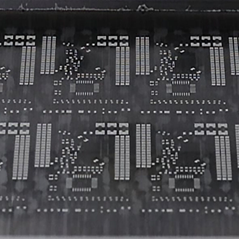
A PCB stencil (also called a solder paste stencil) is a precision-made thin sheet used in surface mount technology (SMT) assembly to deposit accurate amounts of solder paste onto specific pads of a printed circuit board (PCB). It acts as a "mask" that ensures solder paste is only applied where surface mount components will be placed, enabling consistent, high-quality soldering and reducing defects like solder bridges or insufficient solder.
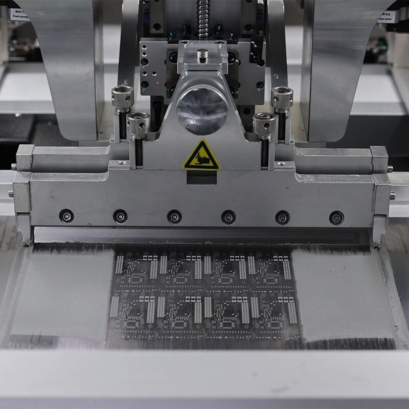
Paste Printing Steps with PCB Stencils
Paste printing (solder paste deposition) is a core surface mount technology process that uses a PCB stencil to apply precise amounts of solder paste onto PCB pads. It directly impacts the quality of component soldering, and follows these 6 standardized steps:
1.Stencil & PCB Preparation
Clean the PCB stencil to remove dust, residual solder paste, or debris from apertures.
Inspect the PCB for surface defects (scratches, oxidation, contamination) and ensure it is dry and static-free.
Match the stencil thickness and aperture size to the PCB’s pad design and component pitch.
2. Precision Alignment
Secure the framed stencil onto the SMT printer’s fixture.
Use optical alignment systems to align the stencil’s apertures perfectly with the PCB’s solder pads.
Confirm alignment accuracy via visual inspection or automated vision checks to avoid offset paste deposition.
3. Solder Paste Setup
Place a suitable amount of solder paste at the starting edge of the stencil.
Ensure the solder paste is at room temperature to maintain optimal viscosity; stir the paste gently if it has settled.
4. Squeegee Printing Process
Set printer parameters: squeegee speed, pressure, and contact angle based on stencil thickness and PCB design.
The squeegee pushes the solder paste across the stencil surface, forcing the paste to fill the apertures and transfer onto the PCB pads.
The stencil is then lifted away from the PCB at a controlled speed (peel speed) to prevent paste smearing or bridging.
5. Post-Print Inspection (PPI)
Conduct 100% inspection of the printed PCB:
Check solder paste volume, shape, and coverage on each pad.
Verify no solder bridges (paste between adjacent pads) or missing paste deposits.
Use automated optical inspection machines for high-volume production, or manual checks for prototyping batches.
Reject or rework defective PCBs immediately to avoid downstream assembly issues.
6. PCB Handling & Transfer
Place the inspected, qualified printed PCBs onto anti-static trays or conveyor belts.
Transfer the PCBs to the component placement stage promptly (within 2–4 hours of printing) to prevent solder paste drying or contamination, which can cause soldering defects during reflow.
Types of PCB Stencils
PCB stencils are precision tools for solder paste deposition in SMT assembly, categorized by fabrication method, structure, and specialized design to fit diverse production needs. Below are the main types and their applications:
Classification by Fabrication Method
| Type | Fabrication Process | Key Advantages | Ideal Use Cases | ||
| Laser-Cut Stencils | A high-power laser ablates apertures on stainless steel sheets; edges can be polished for smoother paste release. | High precision, fast turnaround, cost-effective for medium-to-high volume. | Fine-pitch QFN, BGA, microcontroller PCBs; general SMT production. | ||
| Electroformed Stencils | Nickel is electroplated onto a patterned mandrel to form apertures with smooth, uniform sidewalls. | Ultra-high precision, excellent paste release, no burrs. | High-end electronics; ultra-fine pitch components. | ||
| Chemically Etched Stencils | Stainless steel sheets are coated with photoresist, exposed to UV light via a PCB pattern, then etched with acid to create apertures. | Low cost, simple manufacturing, suitable for standard designs. | Low-volume prototyping, large-pitch components; basic consumer electronics. | ||
Classification by Structure
Framed Stencils
A stainless steel stencil sheet is stretched and mounted onto an aluminum or steel frame.
· Pros: Easy to load into SMT printers, stable alignment, reusable for mass production.
· Cons: Higher cost; less flexible for frequent design changes.
· Use: High-volume SMT assembly lines.
Frame-Less Stencils
A standalone stencil sheet without a frame, often used with reusable stencil holders.
· Pros: Low cost, lightweight, ideal for quick prototyping or small-batch production.
· Cons: Requires manual alignment; not suitable for automated lines.
· Use: R&D, prototype PCBs, small-scale production runs.
Specialized Design Stencils
Step Stencils
Have varying thicknesses across different areas of the stencil.
· Purpose: Solves solder paste volume issues for PCBs with mixed component heights/pitches.
· Use: PCBs with both microchips and large power components.
Flexible Stencils
Made of polyester or thin stainless steel, with flexible properties to fit non-flat PCBs.
· Pros: Conforms to curved or irregular PCB surfaces.
· Cons: Lower durability than rigid stencils.
· Use: Flexible PCBs (FPCs), rigid-flex PCBs.
Magnetic Stencils
Feature magnetic backing to attach to metal frames or printer beds, enabling fast alignment and replacement.
· Pros: Tool-free installation, reduces setup time.
· Use: High-mix, low-volume production lines with frequent stencil changes.
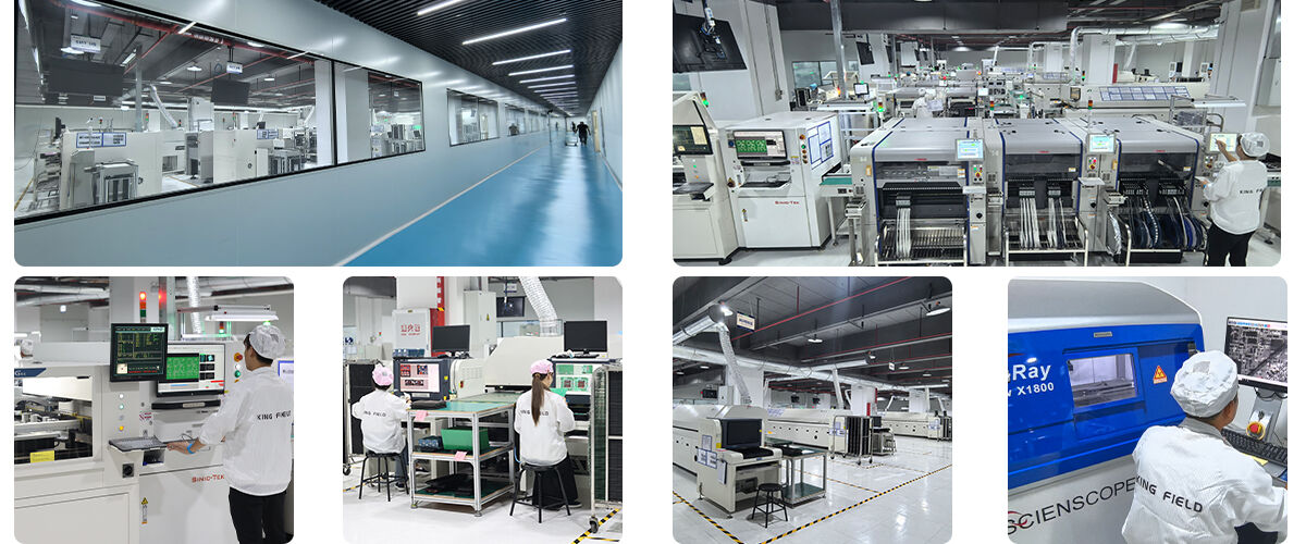
Why choose Kingfield's PCB stencils?
Choose KING FIELD for PCB stencils if you need precision, consistency, fast turnaround, and full SMT integration—backed by 20+ years of SMT/PCBA expertise and a global client base in medical, automotive, and consumer electronics. Below are the core advantages and how they deliver value.
Precision Fabrication for Zero-Defect Printing
· Process Expertise: Laser-cut, electroformed, and chemically etched stencils—matched to your pad design and component pitch.
· Material & Quality: 304 stainless steel and aluminum/steel frames for long-term reuse; strict aperture ratio/width-to-thickness checks to prevent bridging or insufficient solder.
· Alignment & Inspection: Optical alignment systems + post-production AOI/X-ray to ensure 100% aperture-to-pad matching, eliminating offset paste deposition.
Customized Solutions for Complex Designs
· Specialized Stencils: Step stencils (mixed component heights/pitches), flexible stencils, and magnetic stencils.
· Tailored Apertures: Gerber-driven design optimization—circular/rectangular apertures sized to your pads, reducing solder waste and rework costs.
· Prototype to Mass Production: Frameless stencils for R&D, framed stencils for high-volume lines; quick design iterations with 24-hour Gerber processing.
Speed & Cost Efficiency
· Rapid Turnaround: 24-hour technical support, 24-hour file processing, and 48–72-hour production for standard orders.
· Total Cost Savings: Consistent paste deposition cuts rework by 60–70%; durable stencils reduce replacement frequency; no hidden costs for design tweaks.
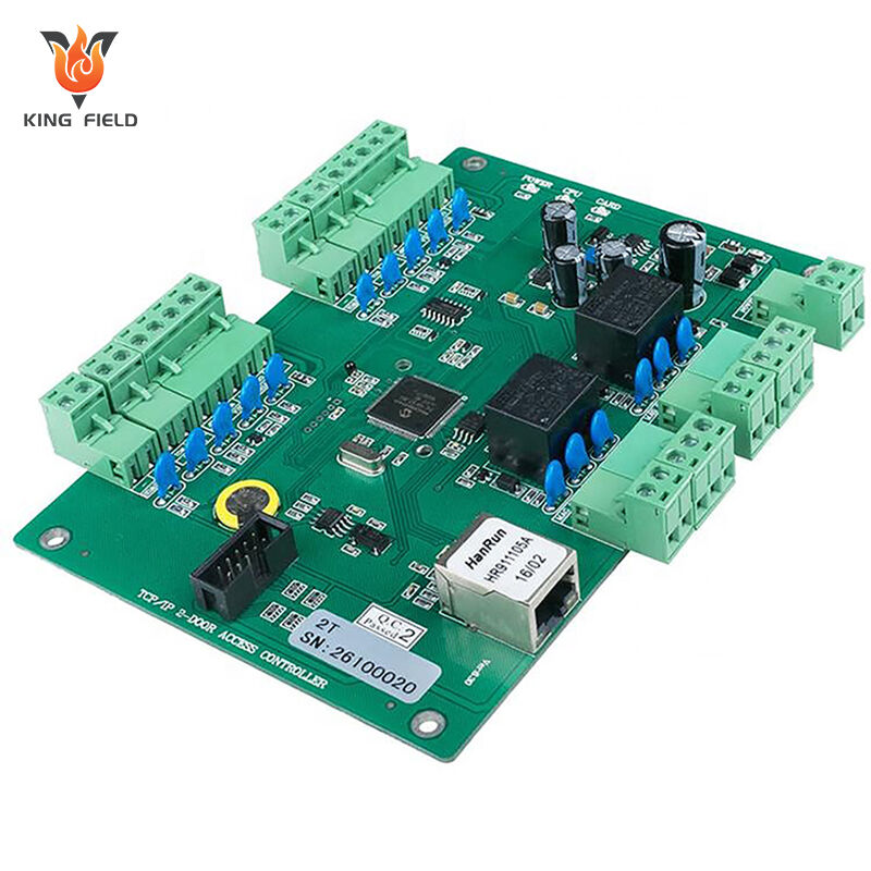
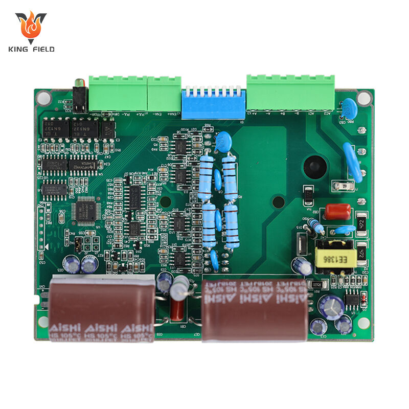
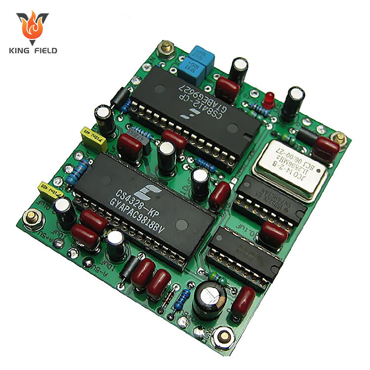
· Seamless Integration: Pair stencils with our full PCBA services for a one-stop solution—no need to coordinate multiple vendors.
Global Service & Support
· Responsive Team: 1-hour response to queries, 24/7 technical help, and dedicated account managers for on-time delivery.
· End-to-End Support: Stencil cleaning guidelines, printing parameter recommendations (squeegee speed/pressure), and post-print inspection protocols to maximize yield.
· Quality Assurance: ISO-certified manufacturing, traceable materials, and batch-to-batch consistency—critical for regulated industries (medical, automotive).