PCB Surface Finish
High-quality PCB Surface Finish solutions for medical, industrial, automotive & consumer electronics. Choose from ENIG, HASL, OSP, Immersion Silver, and Gold Plating—tailored to enhance solder ability, corrosion resistance, and long-term reliability. Precise application, 24h prototyping compatibility, fast delivery, and DFM support ensure optimal performance for your PCBs.
Description
What is PCB surface Finish?
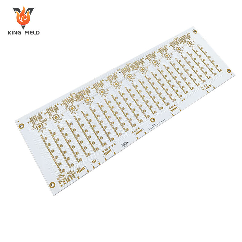
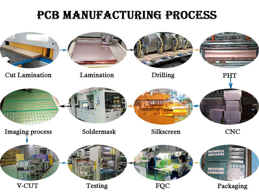
PCB surface Finish is a core post-processing step in PCB bare board production. It refers to depositing a uniform and dense functional coating on the surface of the bare copper layer of the PCB through chemical, physical, or electrochemical methods. Its core function is to solve the pain points of bare copper being prone to oxidation and having poor solderability, while adapting to the performance requirements of different application scenarios. It is a key step in ensuring the soldering reliability, service life, and electrical performance of PCBAs.
Core objective
• Anti-oxidation and corrosion: Bare copper exposed to air and humidity is prone to oxidation, forming copper oxide, which leads to soldering failure and decreased electrical performance. Surface treatment layers can isolate the copper layer from the external environment, extending the storage period and lifespan of PCBAs.
• Improved soldering reliability: The coating must have good wettability to reduce the risk of cold solder joints and false solder joints, especially suitable for the soldering requirements of precision components such as 03015 and QFP in SMT.
• Guaranteed electrical performance: Some coatings can reduce contact resistance and improve signal transmission stability, meeting the performance requirements of high-frequency and high-speed circuits.
• Adaptable to special scenarios: Customized protection is provided for environments with high temperature, high humidity, and high cleanliness.
Common surface treatment types
| Processing type | Process Principle | Core Features | Advantages | limitation | Typical application scenarios |
| HASL | The bare PCB board is immersed in molten solder, and then excess solder is scraped off by high-pressure hot air to form a uniform solder layer. | The solder layer thickness is 5-25μm, and the surface is slightly rough. | Low cost, mature technology, high efficiency in mass production, and strong welding compatibility | The flatness is average, making it unsuitable for fine-pitch components; the high-temperature processing of the lead-free board may affect the PCB substrate. | Consumer electronics, general industrial equipment, power modules |
| ENIG | First, a layer of nickel-phosphorus alloy is chemically deposited, followed by a thin layer of gold plating. The nickel layer acts as a barrier layer, while the gold layer provides solderability and contact performance. | Smooth surface, excellent electrical conductivity, and strong corrosion resistance | It is compatible with precision components and high-frequency circuits, and can be used in contact areas such as buttons and connectors that require repeated insertion and removal. | The cost is relatively high, and excessively thick gold layers can easily lead to "gold brittleness" problems. | High-end communication equipment, medical equipment, automotive electronics, aerospace products |
| OSP | An organic film is formed on the bare copper surface through chemical adsorption, preventing oxidation by air. | The process is environmentally friendly, the surface is smooth, and it does not affect the heat dissipation of the PCB. | Moderately priced, compatible with high-density PCBs and lead-free soldering, the film can decompose naturally after soldering. | High storage environment requirements, generally low temperature resistance | Smartphones, tablets, laptops, IoT devices |
| Immersion Silver | A layer of pure silver is deposited on the bare copper surface through a displacement reaction, resulting in a silver layer with excellent conductivity and solderability. | Low signal transmission loss, good soldering wettability, and high surface smoothness | Lower cost than ENIG, compatible with high-frequency circuits and mid-to-high-end electronic equipment, lead-free and halogen-free, environmentally friendly. | The silver layer is prone to oxidation and its corrosion resistance is slightly inferior to ENIG. | Communication base stations, routers, industrial control modules, and testing instruments |
| Immersion Tin | The displacement reaction deposits a pure tin layer, which has excellent compatibility with solder and can be directly soldered. | Smooth surface, stable welding performance, lead-free and environmentally friendly | It is suitable for assembling fine-pitch and micro-components, with lower process costs than ENIG and a longer shelf life. | The tin layer is relatively soft and easily scratched, so it should be protected from heavy drops or friction. | Automotive electronics, industrial sensors, smart home devices |
Kingfield Surface Treatment Process Advantages
• Full-process quality control: From raw materials to finished products, it complies with IPC-6012 and ISO9001 standards;
• Customized solutions: Recommend the optimal treatment solution according to customer needs, and support special coating customization;
• Environmental compliance: All processes meet RoHS and REACH environmental requirements, are lead-free and halogen-free, and are compatible with the environmental standards of high-end industries such as medical and automotive.
Detailed Process Analysis
Surface treatment processes for different types of PCBs
PCB surface treatment is a core post-processing step in bare board production. It involves forming a functional coating on the copper layer using chemical, physical, or electrochemical methods. This process primarily addresses issues such as bare copper oxidation and insufficient soldering reliability, while also adapting to the performance requirements of different application scenarios. The following is an in-depth analysis of mainstream processes:
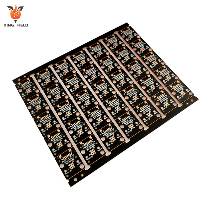
HASL – A cost-effective choice
Process Principle:The bare PCB board is immersed in molten solder, and excess solder is scraped off by a high-pressure hot air knife to form a uniform solder coating on the copper layer surface. After cooling, it solidifies and takes shape.
Core Parameters:
Coating thickness: 5-25μm;
Soldering temperature: 235-245℃ for traditional lead-tin alloys, 250-260℃ for lead-free alloys;
Shelf life: 6-12 months under normal conditions;
Environmental standards: Traditional lead-containing models do not comply with RoHS, lead-free models comply with RoHS/REACH.
Key Features
Advantages: Low cost, mature process, strong soldering compatibility, good wear resistance.
Limitations: Surface flatness is average, not suitable for fine-pitch components; high-temperature processing of lead-free PCBs may cause slight deformation of the PCB substrate.
Typical Applications: Consumer electronics, general industrial equipment, power modules, low-end medical devices.
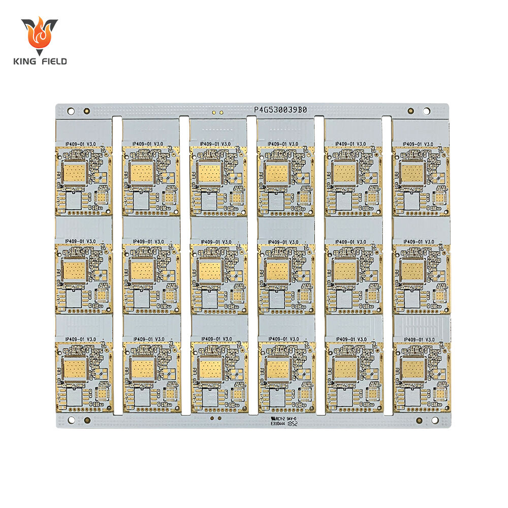
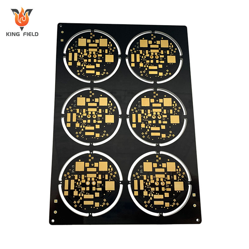
ENIG – The Top Choice for High-End Precision
1. Process Principle
The chemical deposition method is used to first form a nickel-phosphorus alloy barrier layer on the surface of the copper layer, and then deposit a thin gold layer. No electricity is required throughout the process, and the coating has high uniformity
2. Core Parameters
• Nickel layer thickness: 5-10μm, gold layer thickness: 0.05-1.0μm
• Surface roughness: Ra<0.1μm
• Storage period: 12-24 months in a sealed and dry environment
• Corrosion resistance: Salt spray test ≥96 hours (industrial grade), ≥144 hours (military grade)
3. Key Features
Advantages: Smooth surface (suitable for precision components such as BGA and QFP), excellent conductivity, strong resistance to oxidation/corrosion, suitable for high-frequency circuits, supports repeated soldering and insertion/removal.
Limitations: Higher cost, excessively thick gold layers can lead to "gold brittleness," and require high-level process control.
4. Typical Applications High-end communication equipment (5G base stations, optical modules), medical equipment (ventilators, electrocardiographs), automotive electronics, aerospace products, and industrial control precision modules.
III. OSP – High-Density Environmental Solutio.
1. Process Principle
Through chemical adsorption, an ultra-thin organic film is formed on the bare copper surface, isolating it from air and moisture. During soldering, the film can decompose at high temperatures without affecting solder wetting.
2. Core Parameters
Coating thickness: 0.2-0.5μm;
Welding temperature: ≤260℃;
Shelf life: 6-12 months in a dry, sealed environment (humidity > 60% may cause failure);
Environmental standards: Free of heavy metals and halogens, meets RoHS/REACH/IPC-J-STD-004.
3. Key Features
Advantages: Environmentally friendly process, moderate cost, smooth surface, does not affect PCB heat dissipation, no residue after soldering.
Limitations: Moderate temperature resistance, high requirements for storage environment, not resistant to friction.
4. Typical Applications Smartphones, tablets, laptops, IoT devices, high-density PCBs (multilayer boards, HDI boards)
IV. Immersion Silver – A Top Choice for High-Frequency and Mid-to-High-End Products
1.Process Principle:
A pure silver coating is deposited on the surface of a copper layer through a displacement reaction. No electricity is required, and the silver layer is uniform and dense, possessing excellent conductivity and solderability.
2. Core Parameters
• Silver layer thickness: 0.8-2.0 μm
• Surface roughness: Ra < 0.15 μm
• Shelf life: 6-9 months under vacuum packaging
• Conductivity: Contact resistance < 3 mΩ
3. Key Features
Advantages: Low signal transmission loss, good soldering wettability, lower cost than ENIG, lead-free and halogen-free, environmentally friendly, high surface smoothness.
Limitations: Silver layer is prone to oxidation, corrosion resistance is slightly inferior to ENIG, temperature control is required during soldering.
4. Typical Applications:Communication base stations, routers, switches, industrial control modules, testing instruments, and mid-to-high-end consumer electronics.
V. Immersion Tin – A Fine-Pitch Compatible Solution
1. Process Principle
A pure tin coating is deposited on the surface of the copper layer through a displacement reaction. The tin layer is similar in material to solder, has excellent compatibility during soldering, and can directly form reliable solder joints without additional processing.
2. Core Parameters
Tin layer thickness: 1.0-3.0μm;
Surface roughness: Ra<0.15μm;
Shelf life: 6-9 months in a sealed environment;
Soldering temperature: 240-255℃
3. Key Features
Advantages: Smooth surface, stable soldering performance, lead-free and environmentally friendly, lower cost than ENIG/immersion silver, more flexible storage requirements.
Limitations: Softer solder layer, prone to scratches, may develop "solder whiskers" under prolonged high-temperature environments.
4. Typical Applications Automotive electronics, industrial sensors, smart home devices, mid-to-high-end PCBs
VI. Comparison Table of Core Differences in Mainstream Processes
| Comparison Dimensions | HASL | ENIG | OSP | Immersion Silver | Immersion Tin |
| Cost level | Low | high | medium to low | Medium and high | middle |
| Surface flatness | Typical (Ra≈0.8-1.2μm) | Excellent (Ra<0.1μm) | Excellent (Ra<0.2μm) | Excellent (Ra<0.15μm) | Excellent (Ra<0.15μm) |
| Minimum fit spacing | ≥0.5mm pitch | ≥0.3mm pitch | ≥0.2mm pitch | ≥0.4mm pitch | ≥0.3mm pitch |
| Storage period | 6-12 months | 12-24 months | 6-12 months (must be dried) | 6-9 months (vacuum-packed) | 6-9 months |
| Corrosion resistance | Moderate (salt spray ≥ 48 hours) | Excellent (salt spray ≥ 96 hours) | Moderate (salt spray ≥ 48 hours) | Good (salt spray ≥72 hours) | Good (salt spray ≥ 60 hours) |
| Environmental compliance | Lead-free version complies with RoHS | RoHS/REACH compliant | Compliant with RoHS/REACH/Halogen-free | RoHS/REACH compliant | RoHS/REACH compliant |
| Typical application scenarios | General electronics, mass production products | High-end precision, military/medical | High-density consumer electronics, Internet of Things | High-frequency communication, mid-to-high-end equipment |
Automotive electronics, fine-pitch assembly |

