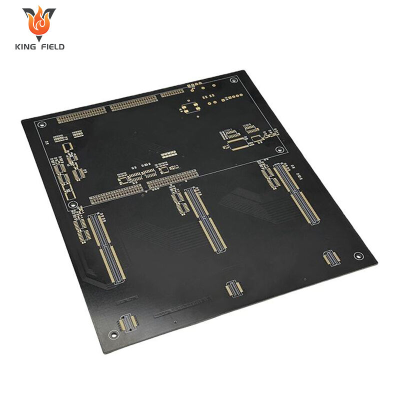
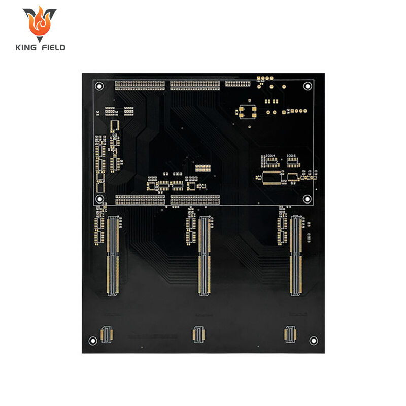
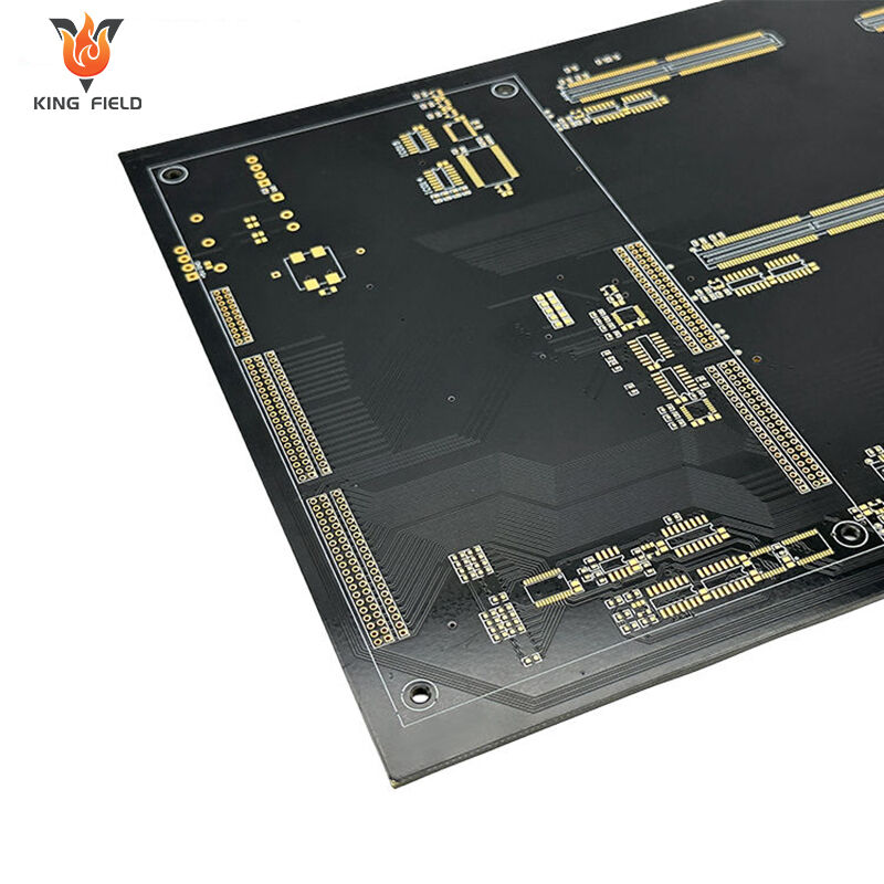
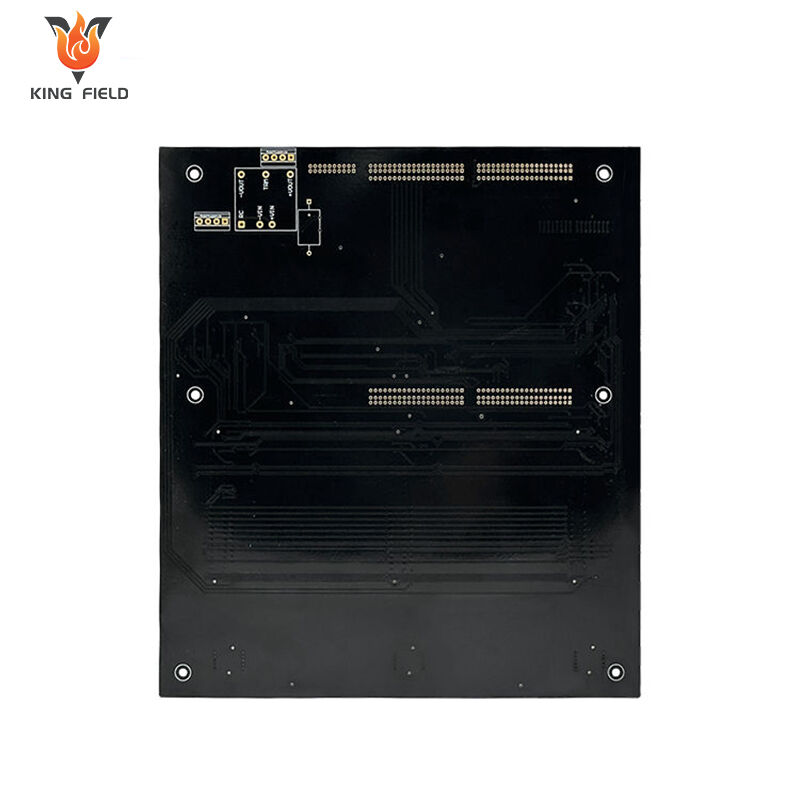
FR4 PCB
Reliable FR4 PCB solutions for medical, industrial, automotive & consumer electronics. High-quality FR4 material, precise fabrication, 24h prototyping, fast delivery, and DFM support + AOI testing. Versatile, cost-effective, and durable—ideal for standard to high-performance applications.
Description
High-Precision FR4 PCBs Lead a New Era in Electronics Manufacturing
Kingfield offers high-quality FR4 PCBs using advanced manufacturing processes, ensuring reliable performance for your electronic devices.
About FR4 PCB
FR4 is a glass fiber reinforced epoxy resin composite material. Due to its excellent balance of mechanical, electrical and thermal properties, it has become the industry standard for printed circuit boards.
What is FR4?
FR4 PCB is a type of printed circuit board made with FR4 material, composed of glass fiber cloth and epoxy resin. It possesses excellent electrical insulation, stable mechanical properties, good chemical resistance, and flame retardancy. Its processing technology is mature and allows for mass production. It is available in various types, including standard, high-TG, and high-CTI, and is widely used in printed circuit boards in consumer electronics, automotive electronics, industrial equipment, and many other fields.
FR4 consists of:
- Glass fiber cloth: provides mechanical strength and dimensional stability;
- Epoxy resin: bonds the glass fibers together and provides electrical insulation;
- Copper foil: forms conductive circuitry on the surface and inner layers.
Product Series
 |
 |
 |
|
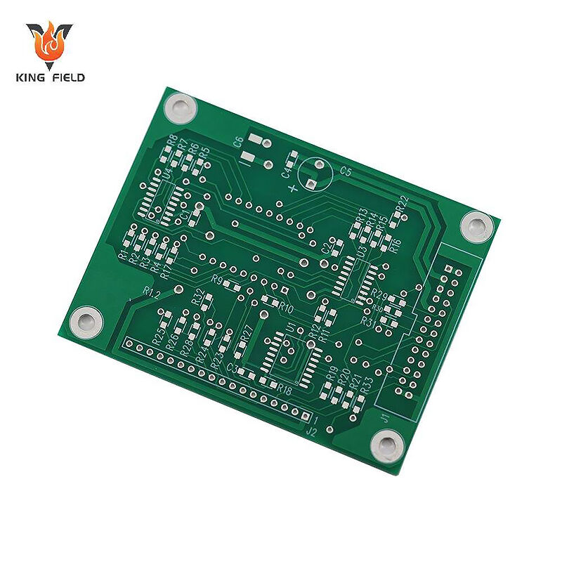
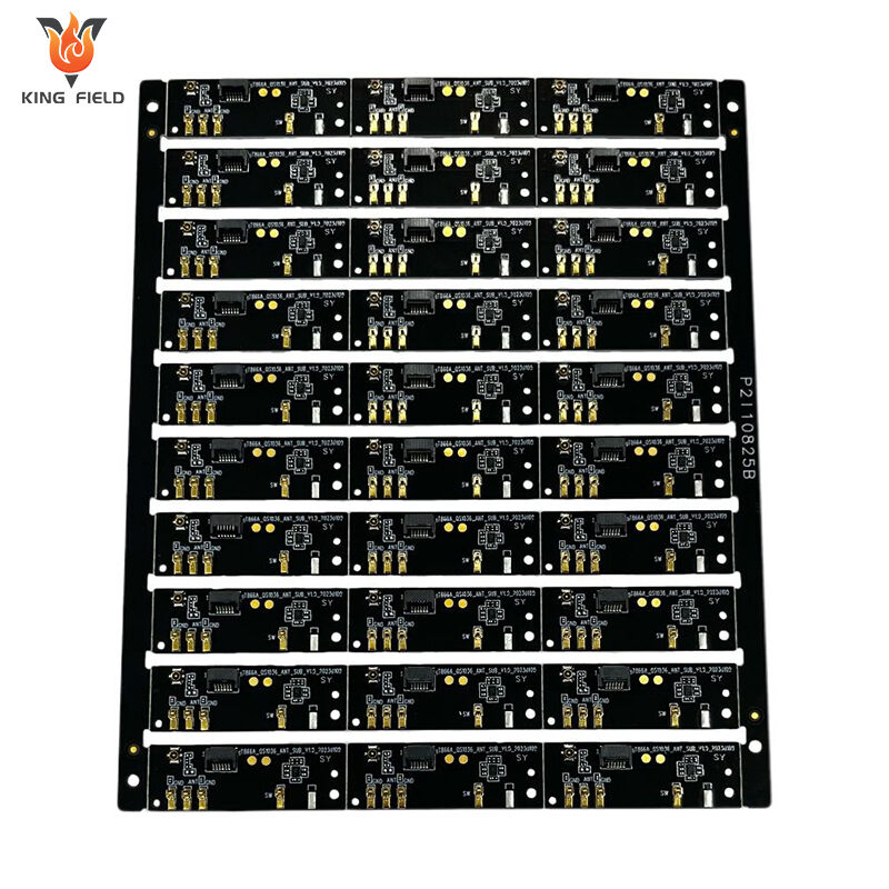
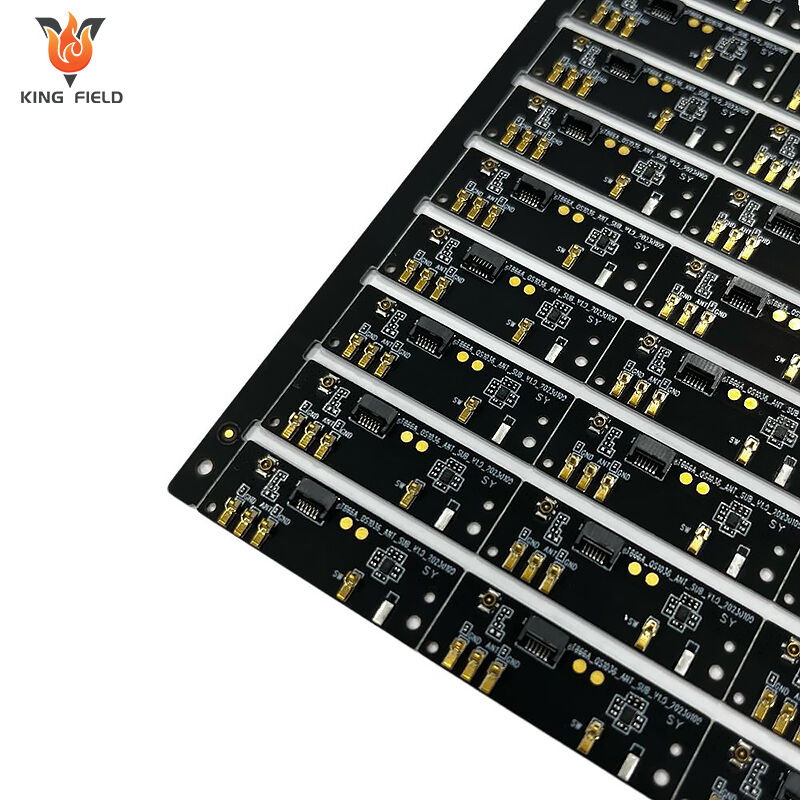
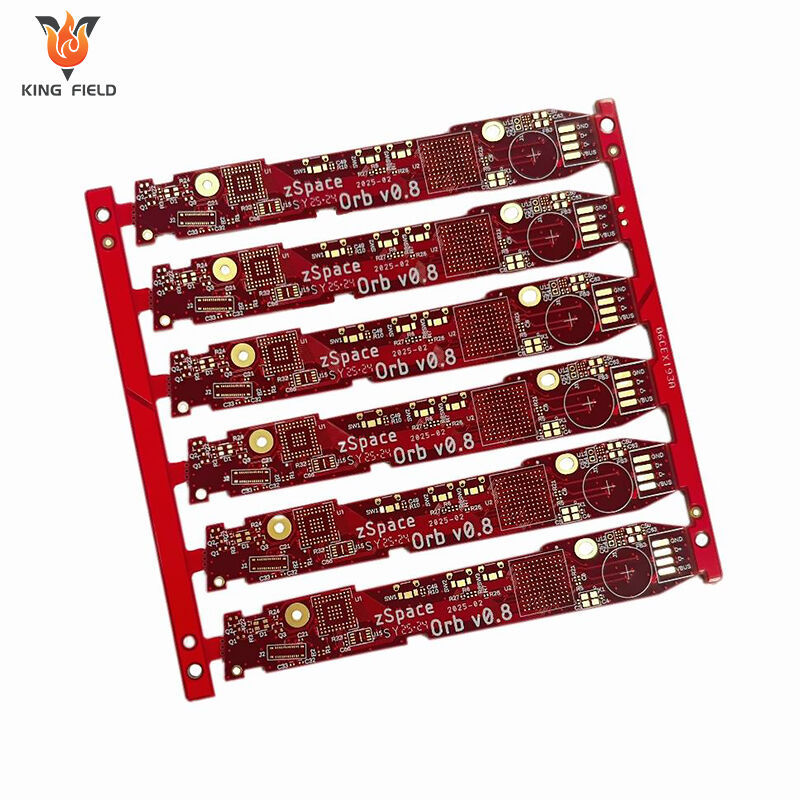
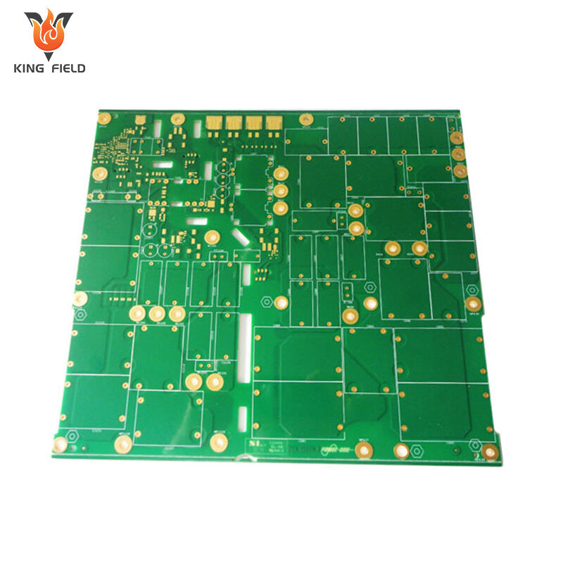
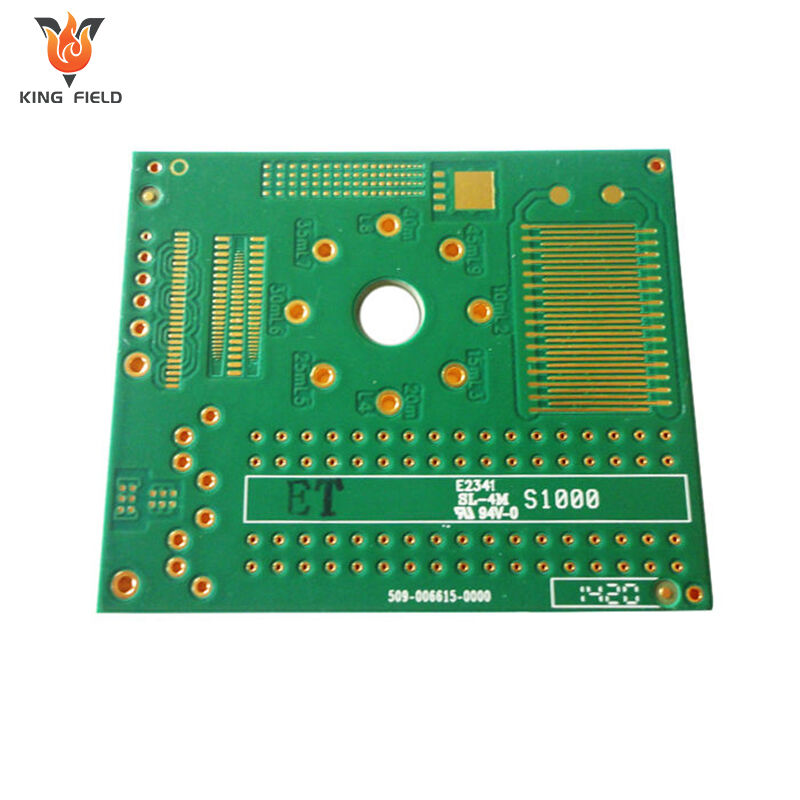
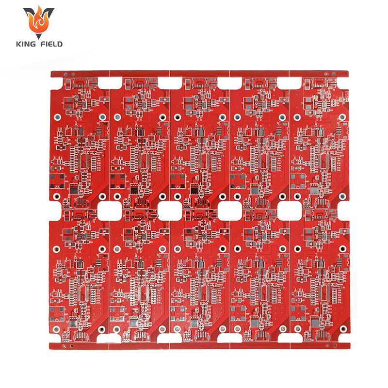
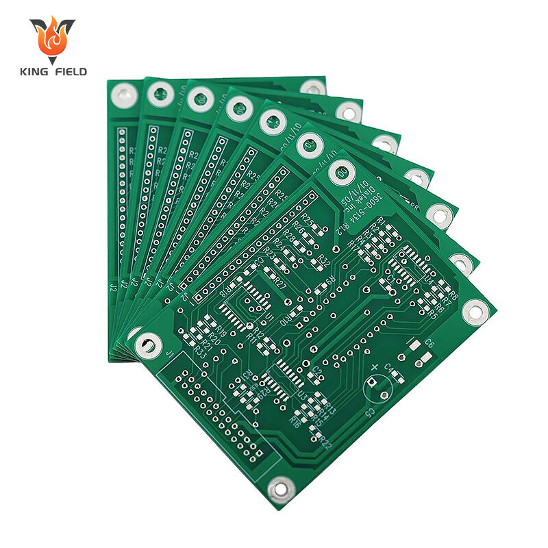
Single-layer FR4 PCB
|
Dual-layer FR4 PCB
|
Multilayer FR4 PCB
|
Technical Features
Technical Features
Kingfield FR4 PCBs utilize advanced technology and stringent quality control to ensure product performance and reliability.
| Made with high-quality FR4 substrate, it has excellent mechanical strength and electrical properties, ensuring stable operation of the circuit board in various environments. | It adopts advanced PCB manufacturing process, supports high-precision circuit design, and the minimum line width/spacing can reach 3mil/3mil. | Each circuit board undergoes rigorous quality testing, including electrical testing, visual inspection, and reliability testing, to ensure product quality. |
| Optimized heat dissipation design and material selection effectively improve the heat dissipation performance of the circuit board, making it suitable for high-power electronic devices. | Low dielectric constant and loss factor, along with excellent impedance control, ensure the stability and reliability of high-frequency signal transmission. | Made with environmentally friendly materials that comply with RoHS and REACH standards, it is environmentally friendly and meets global environmental protection requirements. |
Technical Parameters
| Electrical parameters | Mechanical parameters | Environmental parameters | |||
| Dielectric constant | 4.4 ± 0.2 (1MHz) | Substrate thickness | 0.2mm - 3.2mm | Operating temperature range | -40°C to +130°C |
| Loss factor | < 0.02 (1MHz) | Copper foil thickness | 1/3 oz - 3 oz | Storage temperature range | -55°C to +150°C |
| Volume resistivity | > 10^14 Ω·cm | Minimum line width/line spacing | 1/3 oz - 3 oz | relative humidity | 10% - 90% (non-condensing) |
| Surface resistivity | > 10^13 Ω | Minimum aperture | 0.2mm - 3.2mm | Vibration test | 10-500Hz, 10g, 3-axis |
| Breakdown voltage | > 25 kV/mm | Maximum board size | 600mm × 500mm | Impact test | 50g, 11ms, half-sine wave |
| Maximum operating temperature | 130°C (long-term), 150°C (short-term) | number of floors | Floors 1-20 | Environmental certification | RoHS, REACH |
Applications
|
Applications Kingfield FR4 PCBs are widely used in various industries and fields. |
|||||
| Consumer electronics | Automotive electronics | medical equipment | |||
| Aerospace | Industrial Control | Communication equipment | |||
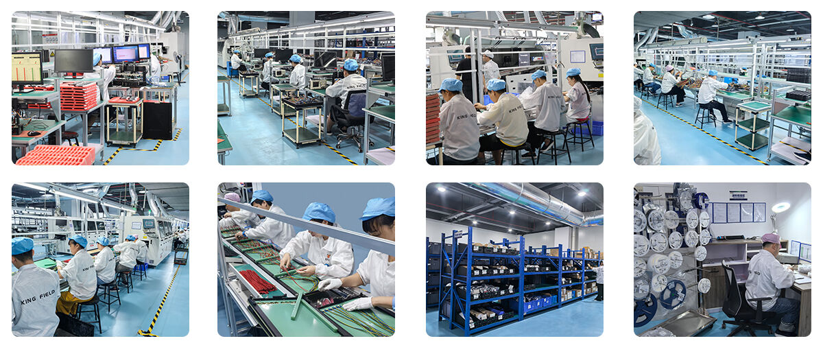
Manufacturing Capacity
| PCB Manufacturing Capability | |||||
| ltem | Production capability | Min space for S/M to pad, to SMT | 0.075mm/0.1mm | Homogeneity of Plating Cu | z90% |
| Layer Count | 1~40 | Min space for legend to pad/ to SMT | 0.2mm/0.2mm | Accuracy of pattern to pattern | ±3mil(±0.075mm) |
| Production size(Min & Max) | 250mmx40mm/710mmx250mm | Surface treatment thickness for Ni/Au/Sn/OSP | 1~6um /0.05~0.76um /4~20um/ 1um | Accuracy of pattern to hole | ±4mil (±0.1mm ) |
| Copper thickness of lamination | 1/3 ~ 10z | Min size E- tested pad | 8 X 8mil | Min line width/space | 0.045 /0.045 |
| Product board thickness | 0.036~2.5mm | Min space between tested pads | 8mil | Etching tolerance | +20%0.02mm) |
| Auto-cutting accuracy | 0.1mm | Min dimention tolerance of outline (outside edge to circuit) | ±0.1mm | Cover layer alignment tolerance | ±6mil (±0.1 mm) |
| Drill size(Min/Max/hole sizetolerance) | 0.075mm/6.5mm/±0.025mm | Min dimention tolerance of outline | ±0.1mm | Excessive adhesive tolerancefor pressing C/L | 0.1mm |
| Min percent for CNC slot length and width | ≤0.5% | Min R corner radius of outline(inner filleted corner) | 0.2mm | Alignment tolerance forthermosetting S/M and UV S/M | ±0.3mm |
| maximum aspect Ratio(thickness/hole diameter) | 8:1 | Min space golden finger to outline | 0.075mm | Min S/M bridge | 0.1mm |

