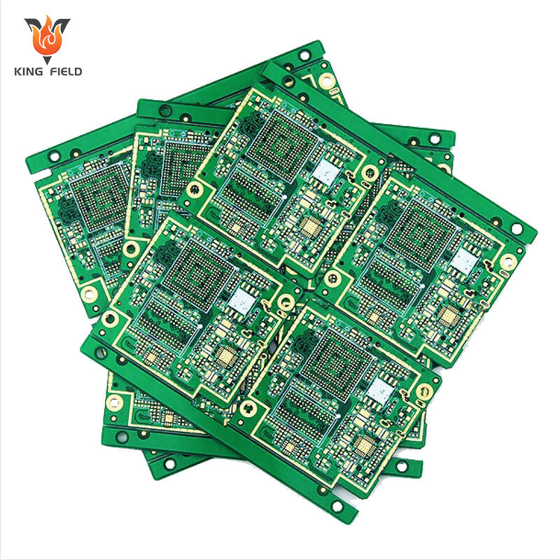
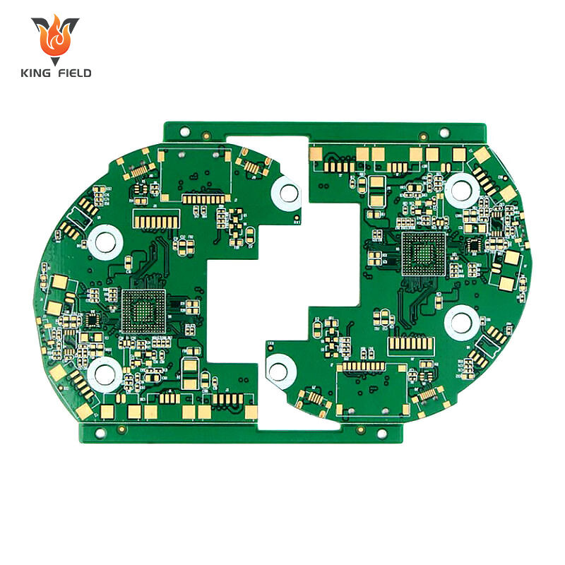
High-TG PCBs
High-TG PCBs engineered for extreme heat & reliability—ideal for medical, industrial, automotive, and high-performance electronics. Heat-resistant materials (high-Tg FR4/PTFE), precise fabrication, 24h prototyping, fast delivery, and DFM support + strict testing. Trust our expertise to power your demanding applications with stable performance under high-temperature conditions.
Description
Meaning of High Tg Printed Circuit Boards
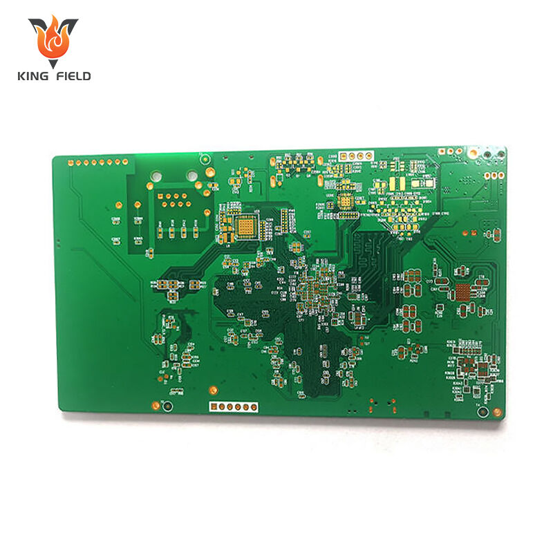
High Tg PCBs use substrate materials with a Tg > 170°C, possessing strong heat resistance, high mechanical stability, and excellent electrical performance. They can withstand high-temperature deformation and solder joint detachment, and are widely used in harsh scenarios such as automotive electronics, aerospace, and high-density circuits. Balancing the requirements of high performance and miniaturization, they are a key choice for improving equipment reliability.
Features of High Tg PCBs Kingfield's High Tg PCB series boasts several core advantages, meeting the demands of high-end electronic devices operating in harsh environments.
• Excellent high-temperature resistance
• Low coefficient of thermal expansion
• Superior electrical properties
• Good flame retardancy
• Strong compatibility
Technical parameters of commonly used materials
We offer a variety of High Tg PCB materials to meet the needs of different application scenarios.
| Material Model | Tg value (°C) | coefficient of thermal expansion | Dielectric constant (1 GHz) | weldability | Application characteristics |
| HT-170 (FR-4) | 170-180 | X:12-16, Y:12-16, Z:60-80 ppm/℃ | 4.4-4.6 | 288℃/10 seconds | High cost-performance ratio, suitable for general industrial equipment |
| HT-180 (IS410) | 180 | X:11-15, Y:11-15, Z:55-75 ppm/℃ | 4.3-4.5 | 288℃/20 seconds | Suitable for multiple temperature cycles and lead-free soldering |
| HT-200 (G200) | 200+ | X:9-13, Y:9-13, Z:45-65 ppm/℃ | 4.2-4.4 | 288℃/30 seconds | High-density multilayer boards, high-performance requirements |
| HT-250 (PI) | 250+ | X:8-12, Y:8-12, Z:40-60 ppm/℃ | 3.8-4.0 | 300℃/30 seconds | Aerospace, extreme environment applications |
| HT-300 (PTFE) | 300+ | X: 5-8, Y: 5-8, Z: 30-50 ppm/℃ | 2.2-2.4 | 350℃/30 seconds | High-frequency microwave, ultra-high temperature environment |
Specification
|
Processing Capabilities
|
||||
High Tg PCBs, with their superior high-temperature resistance, are widely used in electronic devices operating in various high-temperature environments and requiring high performance.
|
Automotive electronics High-temperature applications include engine control units, transmission control systems, and in-vehicle infotainment systems. |
Industrial control Industrial automation equipment, high-temperature furnace control, motor drive systems, and other industrial environments |
Aerospace Extreme environments such as aircraft electronic systems, satellite communication equipment, and navigation systems |
|
Communication equipment 5G base stations, radio frequency modules, high-power amplifiers and other high-temperature operating equipment |
Medical equipment High-temperature sterilization of medical equipment, imaging systems, life monitoring instruments, etc. |
Energy equipment Solar inverters, wind power generation control systems, power conversion equipment, etc. |
Quality control
|
We implement a rigorous quality control process for our High Tg PCB products. From raw material procurement to final product delivery, every step undergoes meticulous testing to ensure product quality meets the most stringent industry standards. This includes: Full compliance with the ISO9001 quality management system; Tg value verification testing for each batch of products; High-temperature cycling testing to ensure product stability; Automated optical inspection (AOI) to ensure circuit accuracy; Compliance with international certification standards such as UL and RoHS. |
 |
||||
Manufacturing capacity
| PCB Manufacturing Capability | |||||
| ltem | Production capability | Min space for S/M to pad, to SMT | 0.075mm/0.1mm | Homogeneity of Plating Cu | z90% |
| Layer Count | 1~40 | Min space for legend to pad/ to SMT | 0.2mm/0.2mm | Accuracy of pattern to pattern | ±3mil(±0.075mm) |
| Production size(Min & Max) | 250mmx40mm/710mmx250mm | Surface treatment thickness for Ni/Au/Sn/OSP | 1~6um /0.05~0.76um /4~20um/ 1um | Accuracy of pattern to hole | ±4mil (±0.1mm ) |
| Copper thickness of lamination | 1/3 ~ 10z | Min size E- tested pad | 8 X 8mil | Min line width/space | 0.045 /0.045 |
| Product board thickness | 0.036~2.5mm | Min space between tested pads | 8mil | Etching tolerance | +20%0.02mm) |
| Auto-cutting accuracy | 0.1mm | Min dimention tolerance of outline (outside edge to circuit) | ±0.1mm | Cover layer alignment tolerance | ±6mil (±0.1 mm) |
| Drill size(Min/Max/hole sizetolerance) | 0.075mm/6.5mm/±0.025mm | Min dimention tolerance of outline | ±0.1mm | Excessive adhesive tolerancefor pressing C/L | 0.1mm |
| Min percent for CNC slot length and width | ≤0.5% | Min R corner radius of outline(inner filleted corner) | 0.2mm | Alignment tolerance forthermosetting S/M and UV S/M | ±0.3mm |
| maximum aspect Ratio(thickness/hole diameter) | 8:1 | Min space golden finger to outline | 0.075mm | Min S/M bridge | 0.1mm |

