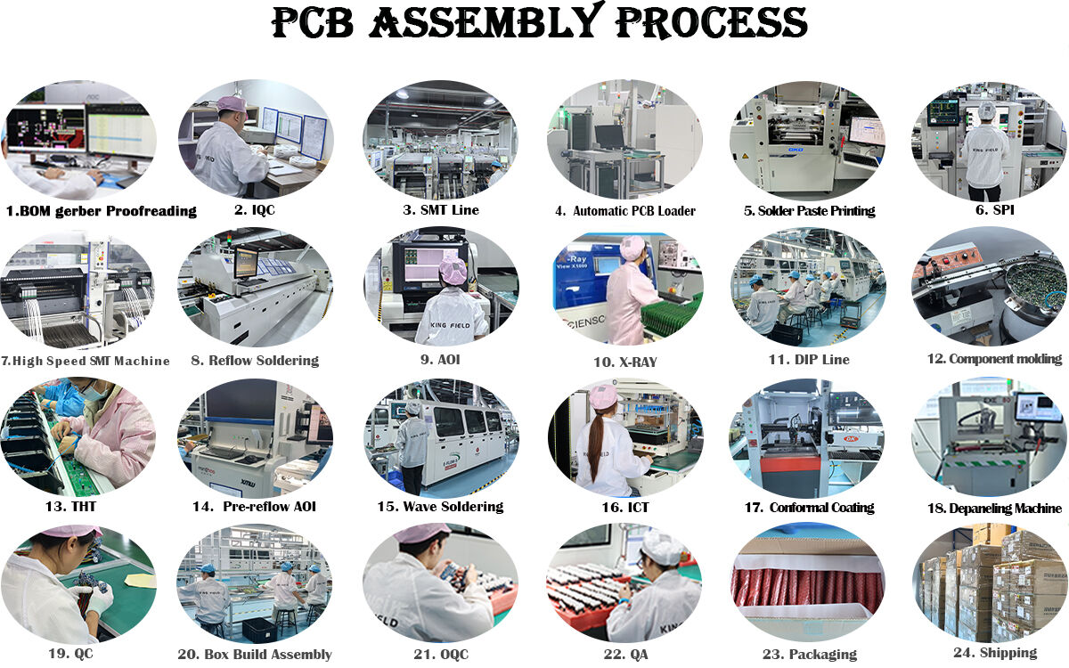
PCB Assembly Process
Streamlined, high-quality PCB Assembly Process for medical, industrial, automotive & consumer electronics. From BOM validation and DFM analysis to component placement, soldering, and AOI/ICT/X-ray testing—we follow strict industry standards for consistent, reliable results.
Our end-to-end process includes rapid prototyping (24h) and scalable mass production, with real-time quality tracking and expert support at every step. Trust our optimized workflow to deliver on-time, defect-free PCB assemblies tailored to your application.
Description
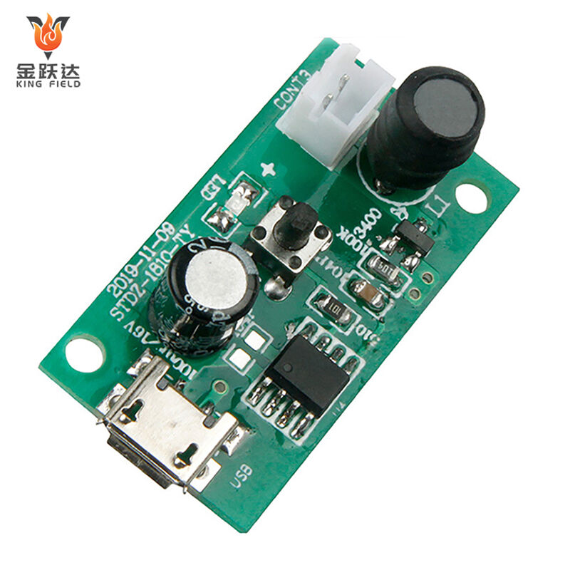
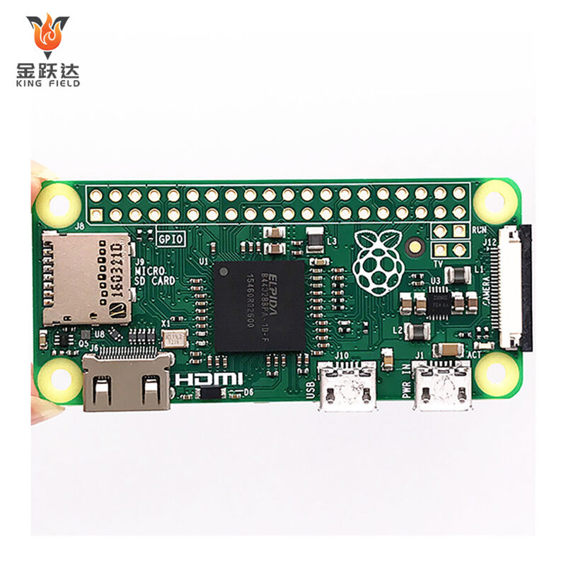
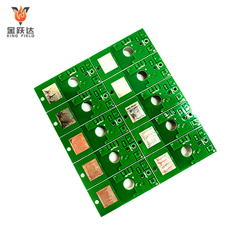
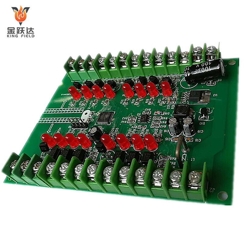
PCB assembly capabilities
We provide cost-effective, one-stop PCBA services – advanced assembly equipment is our core strength. Our current PCB assembly capabilities cover the following areas, and we will continue to maintain our industry-leading position by continuously upgrading our equipment. For needs beyond those listed, please contact [email protected]; we promise a clear response within 24 hours regarding whether we can meet your requirements.
Product Features
| Ability Categories | Specific projects | Technical Specifications/Parameter Range | Notes | ||
| Substrate support | substrate type | Rigid PCB, Flexible PCB (FPC), Rigid-Flex PCB, HDI Board, Thick Copper PCB (Copper Thickness ≤ 6oz) | Supports lead-free/lead-containing substrates, compatible with FR-4, aluminum substrates, Rogers high-frequency boards, and other materials. | ||
| substrate size | Minimum: 50mm×50mm; Maximum: 610mm×510mm (single piece); Panel size ≤ 610mm×510mm | Supports multi-panel disassembly and assembly; the smallest single substrate must meet the mounting and positioning requirements. | |||
| substrate thickness | 0.4mm~3.2mm (standard); custom sizes up to 0.2mm (flexible) / 5.0mm (rigid and thickened) | Thick plates require specialized clamps, while thin plates require anti-deformation treatment. | |||
| Mounting capability | Component type | 01005 (Imperial) ~ 33mm × 33mm Large QFP; BGA, CSP, LGA, POP stacked packages, irregularly shaped components (connectors, sensors) | Supports mounting of ultra-fine pitch components (lead pitch ≤ 0.3mm) and leadless components (DFN, SON). | ||
| Mounting accuracy | Chip components: ±0.03mm; QFP/BGA: ±0.02mm; CSP: ±0.015mm | Employing a vision positioning system, it supports double-sided mounting and stepped mounting (height difference ≤ 2mm). | |||
| Placement speed | Maximum placement speed: 36,000 dots/hour (high-speed machine); Standard capacity: 15,000~25,000 dots/hour | Production capacity is dynamically adjusted according to component complexity and mounting density. | |||
| Welding process | Welding method | Reflow soldering (lead-free/lead-containing), wave soldering (through-hole components), selective wave soldering (partial soldering), manual touch-up soldering | Lead-free solder complies with RoHS standards and supports hybrid processes (some components contain lead, some do not). | ||
| Reflow soldering temperature profile | Maximum peak temperature: 260℃; Number of temperature zones: 10 (4 preheating zones + 2 isothermal zones + 3 reflux zones + 1 cooling zone) | Temperature profiles can be customized based on the temperature resistance characteristics of components (such as connectors and LEDs). | |||
| Plug-in component support | Through-hole resistors/capacitors, DIP packaged ICs, pin headers/female headers, power connectors, transformers, etc., with lead diameter ≤ 1.2mm. | Wave soldering supports a component density of ≤30 dots/square inch. For complex components, selective wave soldering is used to avoid solder bridging. | |||
| Detection capabilities | Appearance inspection | AOI (Automated Optical Inspection) (2D/3D) and manual visual inspection (20x magnifying glass) | AOI inspection has 100% coverage and can identify defects such as cold solder joints, bridging, missing components, and misalignment. | ||
| Electrical testing | Flying probe testing, ICT in-circuit testing, FCT functional testing, X-ray inspection (BGA/CSP bottom solder balls) | Supports customized test fixtures; FCT can simulate the actual working environment of the product to verify its functionality. | |||
| Reliability testing | Temperature and humidity aging test (-40℃~85℃), vibration test, salt spray test (optional) | Reliability test reports can be provided upon request, meeting the requirements of industrial and automotive grade products. | |||
| Special process support | Three-proof treatment | Conformal coating (acrylic/silicone materials), thickness 10~50μm. | Supports localized coating (avoiding connectors and test points), meeting IP65 protection requirements. | ||
| Thermal conductivity treatment | Thermal pad application, thermal paste application, heatsink installation | Suitable for high-power components (such as power ICs and FPGAs) to reduce operating temperature. | |||
| Assembly of irregularly shaped components | Integration and assembly of non-standard components such as batteries, displays, antennas, and metal brackets. | 3D models of the components are required; custom-made fixtures will ensure assembly accuracy. | |||
| Production capacity and delivery time | Mass production capacity | Sample/Small batch: 1~100 sets/day; Medium batch: 100~5000 sets/day; Large batch: 5000~50000 sets/day | Rush orders can shorten delivery time by 30% (process complexity needs to be assessed). | ||
| Standard delivery time | Samples: 3-5 working days; Small batch: 5-7 working days; Medium batch: 7-12 working days; Large batch: 12-20 working days | Delivery time includes the entire process of PCB manufacturing, component procurement, assembly, and testing (assuming components are in stock). | |||
| Quality Standards | Implementation Standards | IPC-A-610E (Acceptability Standard for Electronic Components), IPC-J-STD-001 (Soldering Requirements), RoHS, REACH | Defect rate control: Surface mount defect rate ≤ 0.05%, soldering defect rate ≤ 0.03%, final product qualification rate ≥ 99.5%. | ||
Kingfield's manufacturing capabilities
| Equipment manufacturing process capability | |
| SMT Capacity | 60,000,000 chips/day |
| THT Capacity | 1.500,000 chips/day |
| Delivery Time | Expedited 24 hours |
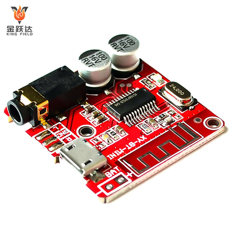
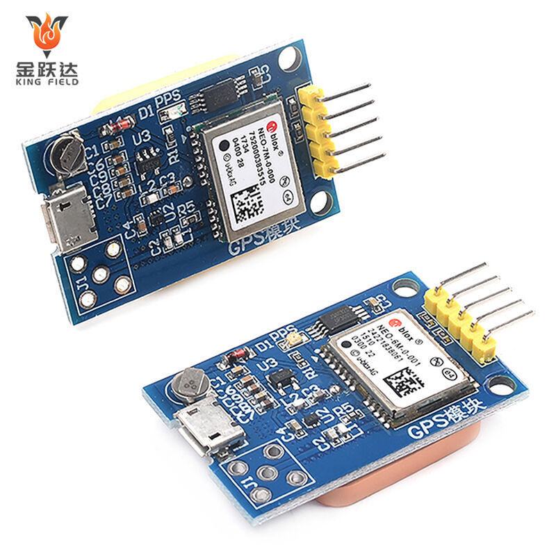
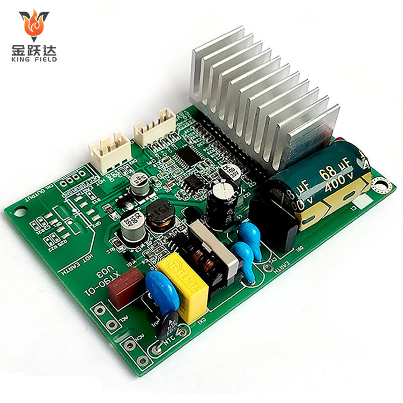
| Types of PCBs Available for Assembly | Rigid boards, flexible boards, rigid-flex boards, aluminum boards |
| PCB Specifications for Assembly |
Maximum size: 480x510 mm; Minimum size: 50x100 mm |
| Minimum Assembly Component | 01005 |
| Minimum BGA | Rigid boards 0.3 mm; Flexible boards 0.4 mm |
| Minimum Fine-Pitch Component | 0.2 mm |
| Component Placement Accuracy | ±0.015 mm |
| Maximum Component Height | 25 mm |

