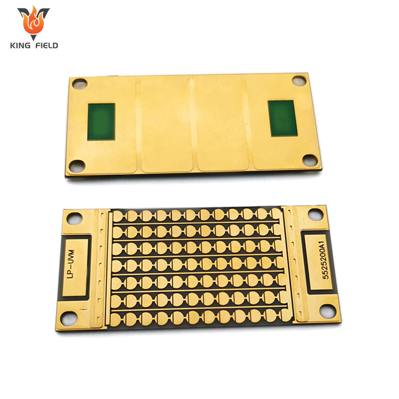
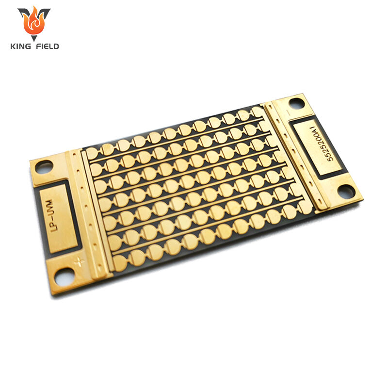
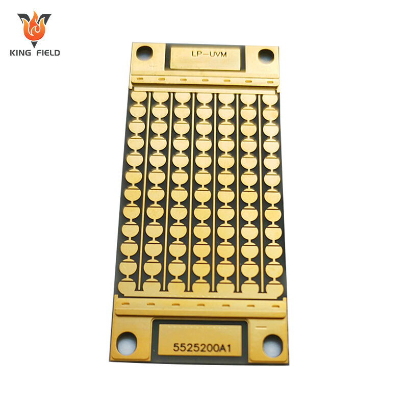
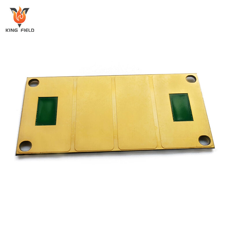
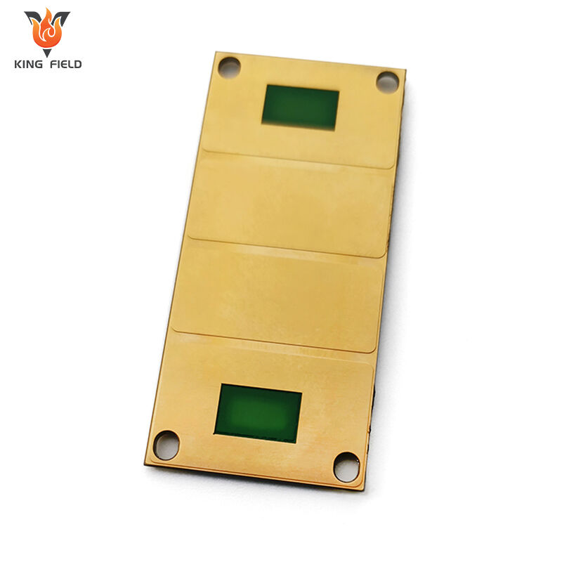
Ceramic PCB
High-performance Ceramic PCBs for medical/industrial/automotive/high-power electronics. Exceptional thermal conductivity, high-temperature resistance & signal integrity. 24h prototyping, fast delivery, DFM support & strict quality testing.
✅ Superior thermal management
✅ High-temperature & corrosion resistance
✅ Precision circuitry for critical applications
Description
What is a ceramic PCB?
Ceramic PCB is a rigid printed circuit board that uses ceramic materials as insulating substrates, such as aluminum oxide Al₂O₃, aluminum nitride AlN, silicon nitride Si₃N₄, etc., and is covered with copper foil to form conductive circuits. It belongs to high-end special PCBS. The core feature is that its thermal conductivity, insulation and high-temperature resistance far exceed those of traditional FR-4 PCBS.
As a high-end special PCB, the core advantages of ceramic PCB are concentrated in key dimensions such as heat dissipation, temperature resistance, insulation and stability, as follows:
· Ultimate heat dissipation performance:
The thermal conductivity of ceramic substrates (especially aluminum nitride) can reach 170-230 W/(m · K), which is more than 500 times that of traditional FR-4 PCBS (about 0.3 W/(m · K)). It can quickly conduct the heat generated by high-power devices, effectively reduce the temperature rise of the devices, and avoid thermal failure. It is compatible with high heat flux density scenarios such as IGBT modules and high-power leds.
· Ultra-high heat resistance:
The long-term operating temperature can reach over 200℃, and the short-term temperature can withstand 500℃, which is far superior to FR-4 PCB (≤130℃). It can adapt to extreme temperature environments such as aerospace and industrial high-temperature equipment without causing deformation or aging of the substrate due to high temperatures.
· Excellent insulation strength:
Breakdown voltage ≥10kV/mm, insulation performance far exceeds that of FR-4 PCB, can work stably in high-voltage circuits, avoid leakage and breakdown risks, and meet the insulation safety requirements of charging piles and high-voltage industrial control equipment.
· Good thermal compatibility:
The coefficient of thermal expansion of ceramic substrates is close to that of semiconductor chips, which can reduce the thermal stress caused by temperature changes, lower the risk of cracking and detachment at the connection between the chip and the substrate, and enhance the reliability and service life of device packaging.
· Chemical and Environmental stability:
Resistant to acids and alkalis, radiation and corrosion. Its performance does not decline in harsh environments such as humidity, strong electromagnetic fields and radiation. It is suitable for special scenarios such as aerospace, Marine exploration and nuclear industry equipment.
· High mechanical strength:
Ceramic substrates have high hardness and strong impact resistance. Especially silicon nitride ceramic circuit board, they can withstand mechanical stresses such as vibration and collision, making them suitable for frequently vibrating working conditions in vehicles and rail transit.
· Low dielectric loss:
Ceramic materials have a stable dielectric constant and low dielectric loss, resulting in small signal transmission loss in high-frequency circuits. They are suitable for high-frequency application scenarios such as 5G base station RF modules and radar equipment.
| Types of ceramic substrates | Types of ceramic substrates | Types of ceramic substrates | Types of ceramic substrates | Types of ceramic substrates | Types of ceramic substrates |
| Alumina (Al₂O₃) | Alumina (Al₂O₃) | Alumina (Al₂O₃) | Alumina (Al₂O₃) | Alumina (Al₂O₃) | Alumina (Al₂O₃) |
| Aluminum nitride (AlN) | Aluminum nitride (AlN) | Aluminum nitride (AlN) | Aluminum nitride (AlN) | Aluminum nitride (AlN) | Aluminum nitride (AlN) |
| Silicon nitride (Si₃N₄) | Silicon nitride (Si₃N₄) | Silicon nitride (Si₃N₄) | Silicon nitride (Si₃N₄) | Silicon nitride (Si₃N₄) | Silicon nitride (Si₃N₄) |
| Beryllium oxide (BeO) | Beryllium oxide (BeO) | Beryllium oxide (BeO) | Beryllium oxide (BeO) | Beryllium oxide (BeO) | Beryllium oxide (BeO) |
| Silicon carbide (SiC) | Silicon carbide (SiC) | Silicon carbide (SiC) | Silicon carbide (SiC) | Silicon carbide (SiC) | Silicon carbide (SiC) |
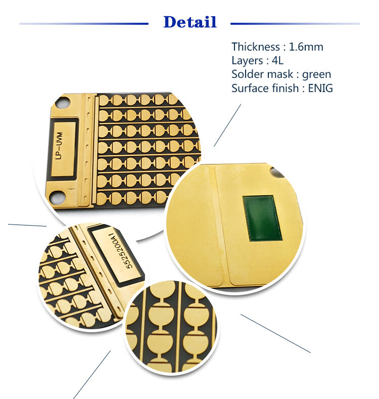
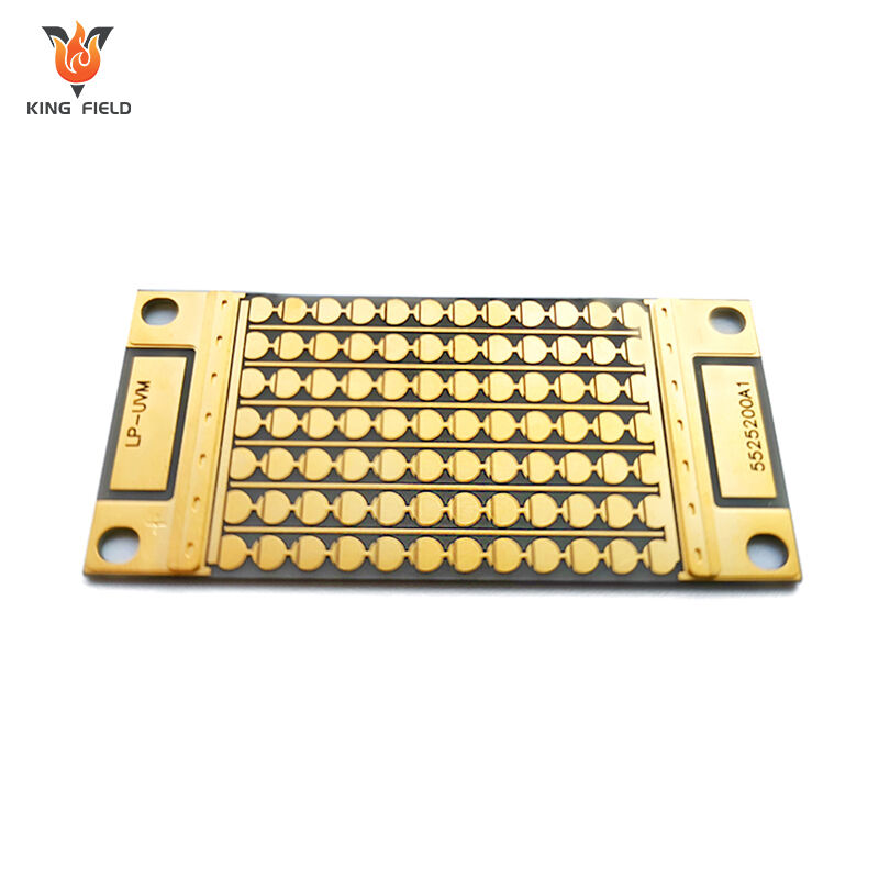
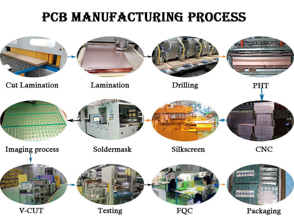
Manufacturing Process
The manufacturing process of ceramic circuit board differs from the etching process of traditional FR-4 PCBS. The core focuses on the reliable combination of ceramic substrates and copper layers. The mainstream processes can be classified into the following categories, each with its own technical characteristics and applicable scenarios:
Direct copper clad lamination process
· Core principle: Copper foil and aluminum oxide/aluminum nitride ceramic substrate are subjected to eutectic welding at high temperatures. The copper-oxygen-ceramic eutectic reaction is utilized to form a metallurgical bonding layer, achieving a firm bond between copper and ceramics.
· Process steps: Ceramic substrate cleaning → copper foil cutting → Copper foil and ceramic lamination → high-temperature vacuum eutectic sintering → cooling → Circuit etching → finished product inspection.
· Key features:
High bonding strength, excellent thermal conductivity (no intermediate bonding layer);
The copper layer thickness has a wide range of options (0.1 to 3mm), and it supports the design of thick copper circuits.
It has good high-temperature resistance and thermal shock resistance, and is suitable for high-power devices.
Disadvantages: High sintering temperature, strict requirements for equipment, only suitable for alumina and aluminum nitride ceramics, not compatible with silicon nitride.
Applicable scenarios: IGBT module substrates, power modules for charging piles, high-power LED substrates.
Active metal brazing process
· Core principle: Between the copper foil and the ceramic substrate, a solder containing active metals such as titanium and zirconium is added. Under a vacuum environment of 800 to 950℃, the active metals undergo a chemical reaction with the ceramic surface to form chemical bonds, while the solder melts to bond the copper foil and the ceramic.
· Process steps: Pretreatment of ceramic substrate → Coating of solder → lamination of copper foil and ceramic → vacuum brazing → Circuit processing → post-treatment.
· Key features:
It has wide adaptability and can be used on all ceramic substrates such as alumina, aluminum nitride, silicon nitride, etc.
The sintering temperature is lower than DBC, causing less damage to the ceramic substrate.
High bonding strength and excellent resistance to cold and hot cycling (no failure after ≥1000 cycles at -40 to 150℃).
Disadvantages: The cost of brazing solder is high, and the process complexity is higher than DBC.
Applicable scenarios: Silicon nitride ceramic PCBS for aerospace, high-reliability power substrates for vehicles.
Thick film process
· Core principle: Metal slurry (silver, copper, palladium-silver alloy) is coated onto the surface of the ceramic substrate through screen printing. After high-temperature sintering, the metal slurry solidifies to form conductive circuits, eliminating the need for copper foil coating.
· Process steps: Ceramic substrate cleaning → Screen printing of metal paste → drying → high-temperature sintering → multiple printing/sintering (thickening the circuit as required) → Insulation layer printing (if multiple layers are needed) → finished product inspection.
· Key features:
The process is flexible, capable of manufacturing fine circuits and supporting multi-layer wiring.
It has a relatively low cost and is suitable for small-batch and customized production.
Disadvantages: The thermal conductivity of the circuit is lower than that of the copper-clad process, the copper paste is prone to oxidation, and the reliability is slightly inferior.
Applicable scenarios: Small sensor circuit boards, high-frequency ceramic pcb board for medical equipment, low-end ceramic substrates.
Low-temperature co-firing ceramic process
· Core principle: Ceramic powder is mixed with organic binders to form raw ceramic tapes. Holes are punched and metal slurry (silver, copper) is filled on the raw ceramic tapes to form circuits/vias. After multiple layers of raw ceramic tapes are stacked, they are co-fired at low temperatures to form multi-layer ceramic PCBS in one go.
· Process steps: Preparation of raw porcelain strips → Drilling → Filling with metal slurry → lamination and stacking → low-temperature co-firing → surface metallization → finished product inspection.
· Key features:
It can achieve high-density multi-layer wiring and integrate passive components (resistors, capacitors) within the substrate.
High dimensional accuracy, with a thermal expansion coefficient matching that of semiconductor chips;
Disadvantages: Complex process, long cycle, high cost, and limited line thickness.
Applicable scenarios: 5G base station RF modules, miniaturized ceramic pcb board for aerospace, high-frequency communication equipment.
High-temperature co-firing ceramic process
· Core principle: Similar to LTCC, but using pure ceramic powder, the sintering temperature is as high as 1500 to 1600℃, and the metal slurry uses high-melting-point metals such as tungsten and molybdenum.
· Key features:
Ceramic has a high density, and its mechanical strength and high-temperature resistance far exceed those of LTCC.
Disadvantages: The sintering temperature is extremely high, the conductivity of the metal slurry is poor, and the cost is expensive.
Applicable scenarios: Extreme high-temperature environments, ceramic PCBS for nuclear industry equipment.
| Process type | Sintering temperature | Core advantage | Main limitations | Typical substrate | |
| DBC | 1065~1083℃ | Excellent heat conduction and moderate cost | Only compatible with alumina/aluminum nitride | Al₂O₃, AlN | |
| AMB | 800~950℃ | It has a wide range of substrate compatibility and high reliability | High cost and complex process | Al₂O₃, AlN, Si₃N₄ | |
| Thick film process | 850~950℃ | Flexible and low-cost | Poor thermal conductivity and prone to oxidation | All ceramic substrates | |
| LTCC | 850~900℃ | High-density integration and high dimensional accuracy | High cost and long cycle | Al₂O₃ -based ceramics | |
| HTCC | 1500~1600℃ | It has extremely high heat resistance and mechanical strength | Poor electrical conductivity and extremely high cost | Pure ceramic substrate | |
Applications of Ceramic PCBs
Ceramic PCBS, with their excellent thermal conductivity, high-temperature resistance and insulation, are mainly applied in high-end scenarios with strict requirements for heat dissipation and reliability. The core fields and specific applications are as follows:
In the field of new energy vehicles
· Core components: Charging pile power module, on-board inverter, motor controller, high-voltage board of battery management system, LED vehicle lamp driver substrate.
· Application reasons:
It can carry large currents, quickly dissipate heat, withstand the alternating high and low temperature environment in vehicles, ensure the stable operation of power devices, and meet the ultra-high thermal conductivity requirements of aluminum nitride ceramic PCBS.
The field of semiconductors and power devices
· Core components: IGBT module substrate, MOSFET packaging substrate, high-power LED heat dissipation substrate, laser diode packaging substrate, RF power amplifier substrate.
· Application reasons: The thermal expansion coefficient of ceramic substrates matches that of semiconductor chips, reducing thermal stress failure. Its thermal conductivity far exceeds that of FR-4, solving the heat dissipation problem of high-power devices. Among them, thick-film process ceramic substrate PCBS are suitable for the mass production requirements of leds.
Aerospace and military industry fields
· Core components: Airborne radar power module, satellite power distribution board, rocket engine control board, missile guidance system circuit board, unmanned aerial vehicle high-power motor drive board.
· Application reasons:
Silicon nitride (Si₃N₄) or HTCC process ceramic PCBS are resistant to extreme temperatures, vibration and shock, and radiation, making them suitable for harsh working conditions in aerospace and military industries.
The field of medical equipment
· Core components: High-frequency electrosurgical knife power substrate, nuclear magnetic resonance (MRI) gradient amplifier board, laser treatment equipment control board, high-voltage power supply module for ventilator.
· Application reasons:
High insulation strength (avoiding leakage risk), high temperature resistance, stable signal transmission, meeting the safety and reliability standards of medical equipment, the cost performance of alumina ceramic PCB is suitable for conventional medical scenarios.
The field of industrial control and high-end equipment
· Core components: High-frequency induction heating equipment substrate, frequency converter power unit, industrial robot servo driver board, high-temperature sensor signal board, photovoltaic inverter power board.
· Application reasons:
Resistant to high temperatures, humidity and vibration in industrial environments, the high thermal conductivity of DBC/AMB process ceramic PCBS ensures the long-term stable operation of high-power industrial control equipment.
The field of 5G communication and radio frequency
· Core components: 5G base station RF power module, millimeter-wave radar substrate, high-frequency board for satellite communication equipment.
· Application reasons:
LTCC process ceramic PCBS can achieve high-density integration and passive component embedding, with low dielectric loss, suitable for high-frequency signal transmission, and at the same time meet the heat dissipation requirements of base station power devices.
Special extreme environment fields
· Core components: Nuclear industry equipment control board, deep-sea exploration robot circuit board, high-temperature industrial furnace sensor substrate.
· Application reasons:
Ceramic PCBS are resistant to radiation, corrosion, and high temperatures. Their performance does not decline in extreme environments such as nuclear radiation, deep-sea high pressure, and high-temperature furnaces. Beryllium oxide ceramic PCBS are suitable for nuclear industry scenarios.
Rigid RPCB Manufacturing Capability
| Item | RPCB | HDI | |||
| minimum linewidth/linespacing | 3MIL/3MIL(0.075mm) | 2MIL/2MIL(0.05MM) | |||
| minimum hole diameter | 6MIL(0.15MM) | 6MIL(0.15MM) | |||
| minimum solder resist opening (single-side) | 1.5MIL(0.0375MM) | 1.2MIL(0.03MM) | |||
| minimum solder resist bridge | 3MIL(0.075MM) | 2.2MIL(0.055MM) | |||
| maximum aspect Ratio (thickness/hole diameter) | 0.417361111 | 0.334027778 | |||
| impedance control accuracy | +/-8% | +/-8% | |||
| finished thickness | 0.3-3.2MM | 0.2-3.2MM | |||
| maximum board size | 630MM*620MM | 620MM*544MM | |||
| maximum finished copper thickness | 6OZ(210UM) | 2OZ(70UM) | |||
| minimum board thickness | 6MIL(0.15MM) | 3MIL(0.076MM) | |||
| maximum layer | 14LAYER | 12LAYER | |||
| Surface treatment | HASL-LF、OSP 、Immersion Gold、 Immersion Tin 、Immersion Ag | Immersion Gold、OSP、selectiveimmersion gold、 | |||
| carbon print | |||||
| Min/max laser hole size | / | 3MIL / 9.8MIL | |||
| laser hole size tolerance | / | 0.1 |