All Categories

What Makes SMT Assembly the Preferred Option for Modern Electronics?

Jan 17, 2026

Introduction: Why Makes SMT Matters Preferred Option in Modern Electronics

The world of electronics manufacturing has witnessed a transformative shift over the past few decades. At the heart of this revolution is Surface Mount Technology (SMT), a process that has propelled the miniaturization of electronics and delivered performance levels that were once unimaginable.

Key Drivers for SMT Adoption

  • Demand for compact devices: Modern electronics—smartphones, smart watches, hearing aids—require densely packed circuits to deliver high performance in small form factors.
  • Assembly line efficiency: The need for faster, more reliable, and scalable production has pushed manufacturers towards automated PCB assembly.
  • Enhanced functionality: SMT enables the integration of more functions per square centimeter, revolutionizing PCB design and expanding device capabilities.
  • Cost pressures: Global competition and consumer expectations for affordable tech have made cost reduction in PCB manufacturing a top priority.

What is Surface Mount Technology (SMT)?

Surface Mount Technology (SMT) is a modern method used for mounting and soldering electronic components directly onto the surface of printed circuit boards (PCBs). Unlike traditional techniques, which relied on inserting component leads through holes in the PCB, SMT allows for direct placement, higher automation, and exceptional circuit density, which significantly benefits electronics manufacturing.

Historical Context: From Through-Hole to Surface Mount

In the 1970s and 80s, electronics manufacturing was dominated by Through-Hole Technology (THT). Components such as resistors, capacitors, and integrated circuits (ICs) were equipped with wire leads that were manually or mechanically inserted into holes drilled into PCBs. This method, while robust, introduced multiple challenges:

  • Manual Labor Intensive: Significant manpower was required for insertion and soldering.
  • Limited Miniaturization: Bulky leads and holes constrained how compact a PCB design could be.
  • Slower Production: Complex products required extensive time for assembly and inspection.
  • Restricted Automation: Full automation was difficult, increasing error rates and labor costs.


Through-Hole Technology (THT)

Surface Mount Technology (SMT)

Component Mount

Leads through drilled holes

Components placed directly on surface

Size

Larger, less dense

Compact, high density

Automation Level

Low to Moderate

Highly Automated

Assembly Speed

Slower

Very Fast

Design Flexibility

Limited

High

The Need for Automation and Efficiency

As the demand for smaller, more efficient, and more powerful electronic devices grew, manufacturers sought ways to pack more circuits onto smaller boards. Automation in PCB assembly became a critical need.

  • Insertions became a bottleneck: Fitting leads through holes—especially as devices shrank—slowed down mass production.
  • Component density hit physical limits: Leads and holes consumed valuable real estate on boards.
  • Inspection and repair were laborious: Manual processes compromised yield and throughput.

Emergence and Dominance of SMT

With SMT, components—called surface-mount devices (SMDs)—are positioned directly onto pads on the PCB's surface. Automated pick-and-place machines precisely position these components at blazing speeds, followed by reflow soldering to secure them.

Key Benefits of SMT’s Emergence:

  • Elimination of drilled holes: Maximizes usable PCB area and supports more compact designs.
  • Rapid automated assembly: Dramatically higher throughput and reduced human error.
  • SMT Components tailored for performance: Optimized for high-frequency, low-power, and minimal parasitics.

SMT vs. Traditional (Through-Hole) Assembly Methods

As electronics manufacturing has evolved, two primary PCB assembly techniques have defined the landscape: Through-Hole Technology (THT) and Surface Mount Technology (SMT). Understanding the nuances, strengths, and weaknesses of both methods is critical for selecting the right approach—or the right mix of methods—for a given application.

Through-Hole Technology (THT): The Benchmark for Robustness

Through-Hole Technology was the backbone of the electronics industry for decades. Here, electronic components with wire leads are inserted into pre-drilled holes on PCBs and then soldered to pads on the board’s underside. This technique delivers certain important advantages:

Strengths of THT Assembly:

  • Mechanical Strength: The leads anchored through the PCB provide strong structural integrity—essential for heavy or high-stress components (e.g., power connectors, transformers).
  • Reliability in Harsh Environments: Particularly valued in automotive, aerospace, and industrial electronics where vibration, thermal cycling, or mechanical shock are concerns.
  • Ease of Manual Assembly and Prototyping: THT is well-suited for hobbyist builds, small-batch production, and scenarios requiring through-hole sockets or larger connectors.

Surface Mount Technology (SMT): The Paradigm of Miniaturization

Surface Mount Technology has rapidly become the standard for modern electronics manufacturing. By mounting components directly on the PCB surface, SMT eliminates the need for drilled holes, enabling revolutionary enhancements:

Strengths of SMT Assembly:

  • High Component Density: Enables extremely compact PCB designs—critical for smartphones, medical implants, and IoT devices.
  • Exceptional Automation: Pick-and-place robotics, high-speed reflow ovens, and automated optical inspection (AOI) deliver speed, accuracy, and high production yields.
  • Faster Assembly Line Efficiency: Eliminating manual insertion and multi-step soldering slashes production times.
  • Superior Electrical Performance: Shorter, more direct conductive paths reduce unwanted inductance and capacitance, making SMT ideal for high-frequency electronics.
  • Support for Miniaturization: Smaller package sizes support the ongoing shrinkage of electronic devices.
  • Lower Power Dissipation: SMT resistors and capacitors typically have reduced power ratings and improved heat management due to shorter leads and optimized packages.

Comparative Quick Reference Table

Criteria

Through-Hole Technology (THT)

Surface Mount Technology (SMT)

Mounting Method

Leads through drilled holes

Components on PCB surface

Component Size

Larger, bulkier

Small, compact

Circuit Density

Low

High

Assembly Speed

Slow

Fast (highly automated)

Mechanical Strength

High (for large components)

Limited (best for small devices)

Electrical Performance

Limited at high frequency

Superior for high-frequency

Automation

Moderate to difficult

Extensive; easily automated

Prototyping

Easy

More challenging

Typical Use Cases

Industrial, Aerospace, Auto (power parts)

Consumer, Mobile, IoT, Medical

The Case for Mixed-Technology PCB Assembly

Increasingly, mixed-technology PCB assembly—combining both SMT and THT—offers the best of both worlds:

  • Use SMT for high-density, high-speed signals and compact areas.
  • Use THT for components that require mechanical strength or high current handling.

配图1.jpg

Core Advantages of SMT Assembly in Electronics Manufacturing

The transition to Surface Mount Technology (SMT) has ushered in a new era for the electronics industry. SMT assembly brings a wide array of advantages, transforming virtually every stage of PCB manufacturing, from design efficiency and component density to cost-effectiveness and reliability. Let’s dive deep into these core benefits and examine why SMT assembly is now the standard in modern electronics manufacturing.

1. Higher Assembly Efficiency and Automation

One of the most transformative advantages of SMT assembly is the ability to leverage automation for unparalleled speed and consistency:

  • Automated Placement of Components: Using advanced pick-and-place machines, thousands of surface-mount components can be precisely positioned on a PCB within minutes.
  • Streamlined Soldering Process: The reflow soldering technique allows entire boards to be soldered at once, further boosting throughput and yield.
  • Reduction in Human Errors: Full-scale automation minimizes the risk of soldering defects, misaligned components, or incorrect orientation.

2. Compact PCB Design and Higher Component Density

SMT components are drastically smaller than their through-hole counterparts. Their small footprints empower engineers to design high-density circuits, enabling more complex functionality in minimal board real estate.

Benefits of High Component Density:

  • Miniaturization of Electronics: Today’s smartphones, wearables, and IoT devices are possible only due to compact SMT assemblies.
  • Multi-layer PCB Support: SMT allows for seamless multi-layer stackups, offering advanced routing for complex designs.
  • Enhanced Design Flexibility: Smaller SMT packages (like 0402 or 0201 for resistors/capacitors) enable designers to fit a broader range of features or higher speeds in confined spaces.

3. Lower Power Ratings & Improved Performance

SMT resistors and capacitors typically offer lower power dissipation due to their minimal sizes and optimized conductor lengths. Additionally, surface-mount configurations enable:

  • Lower electrical path inductance and capacitance: Shorter connections reduce parasitic elements, making SMT ideal for high-frequency and high-speed circuits.
  • Better thermal performance: Efficient thermal management and stronger heat resistance in modern SMT packages reduce the risk of overheating.

4. Cost Reduction in PCB Manufacturing

Cost efficiency is among the top drivers for SMT adoption, impacting both small-scale and large-volume manufacturers:

  • Fewer Drilled Holes: Direct surface mounting eliminates expensive and time-consuming drilling steps.
  • Reduced Material Costs: Smaller packages mean less material per component.
  • Lower Labor Costs: Automation streamlines the PCB assembly process, reducing manual labor requirements significantly.
  • Consistent Quality: Fewer defects and reworks lead to higher overall yield rates.

Table: Estimated Cost Comparison (Typical Values)

Assembly Method

Per Board Labor Cost

Component Cost

Equipment Cost (per unit, amortized)

Yield Rate

THT (Manual)

High

Standard

Low

92%

SMT (Automated)

Very Low

Lower

Moderate/High

98%

5. Enhanced Reliability and Improved Performance

  • Uniform Solder Joints: Automated reflow processes create consistent, reliable connections that are less prone to failure than hand-soldered joints.
  • Better High-Frequency Characteristics: The short surface paths of SMT lead to improved high-frequency signal integrity and reduced electromagnetic interference.
  • Lead-Free Compatibility: SMT is more easily adapted to lead-free soldering standards, supporting environmental and regulatory compliance.

6. Full Compatibility with Mixed & Hybrid Assemblies

While SMT has largely replaced through-hole in consumer electronics, one of its less discussed strengths is coexistence with through-hole circuit boards in hybrid or mixed-technology PCB assemblies. Manufacturers can optimize each design using the best of both worlds—for example, combining surface-mount microcontrollers with through-hole connectors for better power handling and physical durability.

7. Unmatched Scalability for Mass Production

Once a PCB design is ready, SMT assembly lines can be scaled nearly infinitely—serving both mass production for consumer electronics and the demanding quality standards of medical and aerospace PCB manufacturing.

Key Takeaways:

  • Optimal for high-volume runs.
  • Suited for complex, multilayer, and compact boards.
  • Provides the agility needed for competitive electronics markets.

8. Improved Reliability and Consistency over Time

Because SMT assembly relieves the process from most human intervention, SMT circuits offer longer lifespans, greater consistency, and superior overall reliability. Coupled with built-in self-test features and automated optical inspection (AOI), failure rates are significantly minimized.

SMT Advantages: A Quick-Reference List

  • High-density circuit design
  • Seamless automation and scalability
  • Faster assembly and shorter time-to-market
  • Lower total manufacturing and labor costs
  • Superior high-frequency and signal performance
  • Smaller, lighter, and more integrated product designs
  • Environmentally friendly, supporting lead-free standards

Exploring SMT Components & Devices

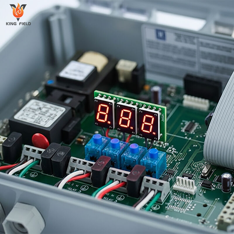
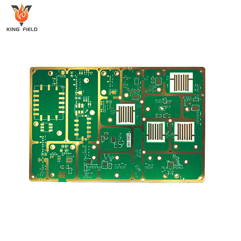
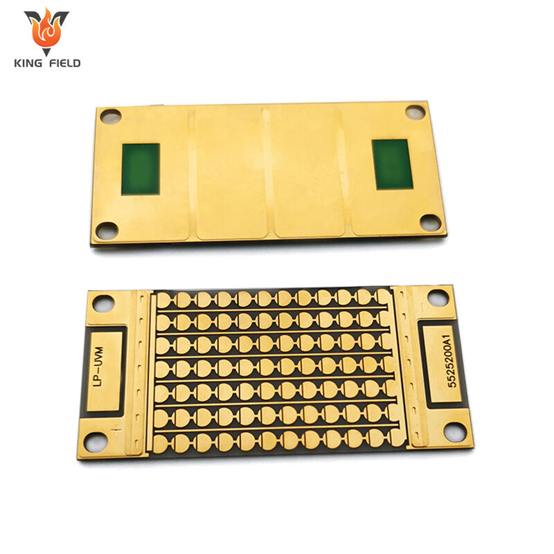
Surface Mount Technology (SMT) has allowed the development of a vast range of specialized electronic components tailored for highly automated, high-density PCB assembly. Their unique physical characteristics and packaging have directly contributed to the miniaturization of electronics and the fulfillment of complex design requirements in modern devices. In this section, we’ll take an in-depth look at the kinds of SMT components, their package styles, and how they differ from traditional through-hole counterparts.

SMT Components vs. Through-Hole Components

The fundamental difference between surface-mount and through-hole components lies in how they connect to the printed circuit board (PCB):

  • Through-hole components have wire leads that are inserted into plated holes and soldered on the opposite side.
  • SMT components (or surface-mounted devices, SMD) have metallic terminations or leads that sit directly atop PCB solder pads and are affixed using reflow soldering.

Key Differences

Feature

SMT Components

Through-Hole Components

Mounting Method

On PCB surface

Through PCB holes

Package Size

Very small, compact

Typically larger

Assembly

Fully automated possible

Mainly manual/semi-automated

Signal Performance

Low parasitics, high speed

Higher inductance/capacitance

Application

High-density/compact

Mechanical strength required

Major SMT Package Types

1. Passive Components: Resistors and Capacitors

SMT resistors and capacitors come in standardized, miniature packages designed for quick identification by automated assembly equipment:

Common SMT Size Code

Metric Size (mm)

Typical Use Cases

1206

3.2 × 1.6

Power, less dense boards

0805

2.0 × 1.3

Mixed-density designs

0603

1.6 × 0.8

Consumer electronics

0402

1.0 × 0.5

High-density, mobile

0201

0.6 × 0.3

Ultra-compact, IoT

2. Integrated Circuits (ICs)

SMT has enabled the packaging and assembly of highly complex ICs, such as microcontrollers, FPGAs, and memory chips.

Popular SMT IC Packages:

Package Type

Abbreviation

Pin Count Range

Typical Width (mm)

Example Application

Small Outline Integrated Circuit

SOIC

8–50

3.9–12.8

Logic, drivers

Quad Flat Package

QFP

32–256

9–32

Microcontroller, DSP

Ball Grid Array

BGA

32–1000+

5–35

CPUs, FPGAs

Chip Scale Package

CSP

8–100+

2–10

Mobile processors

3. Discrete Semiconductors: Transistors and Diodes

Discrete semiconductors are now most commonly supplied in tiny plastic packages for surface mounting, enhancing both automation and board efficiency.

Common Packages:

  • SOT-23, SOT-223: Widely used for bipolar transistors, FETs, and voltage regulators.
  • SOD, MELF: For diodes and specialty passive components.

4. Additional SMT Component Types

  • Inductors: Available as tiny chips or wirewound packages for RF and power supply circuits.
  • Connectors: Even some miniaturized connectors now come in hybrid or full SMT variants, optimized for automated placement but still providing mechanical robustness.
  • Oscillators & Crystals: SMT variants simplify high-speed timing integration.

SMT Component Orientation & Placement

High-speed pick-and-place machines read component feeders, orient each part precisely, and place it on solder-pasted pads. This precision ensures maximum PCB yield rate and repeatability, minimizing risks tied to human handling.

Common Placement Considerations

  • Component Orientation: Ensures pin 1 or polarity marks align with PCB layout—critical for ICs and polarized capacitors.
  • Thermal Resistance: SMT components are engineered for high thermal cycling and can survive the intense heat of reflow ovens.
  • Component Coding: Clear markings and standardized codes help automated optical inspection (AOI) systems verify correct placement.

Table: SMT Package Reference Summary

Category

Examples (Package)

Typical Size Range

Assembly Method

Resistors

0201, 0402, 0603

0.6mm–1.6mm

Automated, solder paste & reflow

Capacitors

0402, 0805, 1206

1.0mm–3.2mm

Automated, solder paste & reflow

ICs

SOIC, QFP, BGA, CSP

3.9mm–35mm

Automated, solder paste & reflow

Transistors

SOT-23, SOT-223

1.2mm–6mm

Automated, solder paste & reflow

Diodes

SOD, MELF

1.0mm–5mm

Automated, solder paste & reflow

Inside the SMT Assembly Process: Step-by-Step

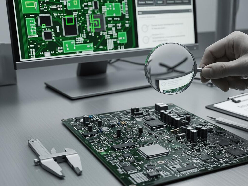
The SMT assembly process is a sophisticated, highly automated series of steps that integrates mechanical precision, chemistry, and computer vision to reliably produce high-quality printed circuit boards (PCBs). The entire workflow is designed to maximize reliability, signal integrity, and production throughput, making it the heart of modern electronics manufacturing. Below, we’ll dissect each major phase, exploring the advanced machinery, process checks, and resulting SMT advantages.

1. Solder Paste Application

The journey of an SMT board begins with the application of solder paste to the bare PCB’s pads.

Solder Paste is a mixture of tiny solder particles and flux. It serves as both the adhesive for holding components during placement and the actual solder for permanent bonding during the reflow process.

Key Steps:

  • stainless steel stencil—custom-cut to match the pad layout—is placed over the PCB.
  • Automated screen printers apply solder paste through the stencil's openings, coating each pad with a precise deposit.
  • Advanced machines verify the volume and location of each paste deposit using solder paste inspection (SPI) systems.

2. Component Placement (Pick-and-Place Technology)

Next, state-of-the-art pick-and-place machines spring into action:

  • Component Feeders: Each SMD (surface-mount device) component is loaded into the machine using reels, tubes, or trays.
  • Vision Systems: Camera-guided head assemblies pick up components using pneumatic suction, verify orientation, and ensure size and type.
  • High-Speed Placement: The automated placement head positions each component onto the freshly pasted PCB at rates of tens of thousands of placements per hour.

3. Reflow Soldering: The Heart of SMT Joining

Perhaps the most vital and unique feature of SMT assembly, reflow soldering is where the temporary bonds of solder paste become reliable, permanent electrical and mechanical connections.

Process Phases in Reflow Soldering:

Phase

Temperature Range

Main Purpose

Duration

Preheat Zone

130–160°C

Gradually heat PCB, activate flux

60–120 sec

Soak Zone

160–200°C

Evaporate volatiles, wetting solder

90–120 sec

Reflow Zone

220–250°C

Melt solder, form joints

30–60 sec

Cooling Zone

~150°C → ambient

Solidify solder, stabilize joints

60–120 sec

  • Thermal Profiles are optimized for component and PCB type, preventing damage to sensitive SMT packages.
  • Boards pass through automated reflow ovens with precisely controlled heat gradients.

4. Automated Optical Inspection (AOI) & Quality Checks

Upon exiting the reflow oven, PCBs are rapidly routed to automated optical inspection (AOI) stations:

  • AOI uses high-resolution cameras to compare each assembled board against pre-programmed references, checking for misplaced, missing, or misoriented components as well as solder joint integrity.
  • Advanced AOI systems analyze thousands of features per board in seconds, detecting defects invisible to the naked eye.
  • In many lines, X-ray inspection is used for highly complex packages (such as BGAs) to identify hidden defects like voids, insufficient solder, or shorts beneath the package.

Additional Quality Steps

  • Functional Testing: On high-value or safety-critical PCB assemblies, inline or end-of-line functional test stations validate performance under simulated operating conditions.
  • Manual Review: Occasionally, flagged boards are reviewed by skilled technicians for rework or corrective action.

5. Final Cleaning and Preparation

Even lead-free, clean-process soldering can leave microscopic residues. With high-reliability boards (medical, automotive, aerospace), automated washing and drying systems remove all leftover flux or particulate matter to guard against corrosion and signal leakage.

SMT Assembly Process Flow—Summary Table

Step

Equipment Involved

Automation Level

Quality Control

Solder Paste Application

Screen printer, SPI

Fully automated

Solder Paste Inspection (SPI)

Component Placement

Pick-and-place machine

Fully automated

Vision-guided precision

Reflow Soldering

Reflow oven

Fully automated

Thermal profile validation

Inspection & Testing

AOI, X-ray, in-circuit testers

Mainly automated

Defect detection, performance tests

Cleaning/Finishing

Wash/dry station

Partially automated

Ionic contamination testing (if needed)

Case Study: Scaling Up for Modern Production

A global consumer electronics manufacturer uses SMT lines to produce smartphone PCBs. Each line:

  • Operates 24/7 with minimal human intervention
  • Achieves over 99.9% yield rate on 10,000+ boards per shift
  • Automatically detects and resolves issues in real-time, ensuring uniform quality

The Role of Human Expertise

While SMT assembly emphasizes automation, human engineers and technicians are critical for:

  • Programming pick-and-place and inspection systems
  • Troubleshooting unexpected process errors
  • Designing new boards for manufacturability (see DFM, next section)

Summary

The SMT PCB assembly process exemplifies how synergy among advanced tools, rigorous process controls, and expert oversight leads to precision soldering, extremely high yield rates, and exceptional product reliability—attributes that define today’s best electronics manufacturing.

The Mixed-Technology PCB Advantage (SMT + THT)

While Surface Mount Technology (SMT) dominates the landscape of modern electronics manufacturing, Through-Hole Technology (THT) remains indispensable for numerous high-reliability or high-stress applications. By harnessing the strengths of both, engineers have developed mixed-technology PCB assembly—a hybrid approach unlocking new heights of design flexibility, reliability, and performance.

What is Mixed-Technology PCB Assembly?

Mixed-technology PCB assembly involves strategically combining SMT components and traditional THT components on a single circuit board. This method enables manufacturers to exploit the advantages of miniaturization, automated placement, and cost savings of SMT while retaining the mechanical robustness and power-handling capacity provided by THT components.

Key Benefits:

  • Optimizes space and performance: Dense, high-speed logic and signal lines use SMT, while heavy loads and connectors leverage THT.
  • Improves board reliability: Critical mechanical mounts (power connectors, relays) withstand vibration, impact, and repeated stress.
  • Enables multi-functionality: Supports complex multi-layer PCB layouts for advanced automotive, aerospace, industrial, and medical applications.

Workflow of a Mixed-Technology PCB Assembly

Step-by-Step Mixed Assembly Process

Step

SMT Process

THT Process

Automation Level

1

Solder Paste Printing (for SMT pads)

Holes drilled, pads plated

Automated (SMT), Semi-automated (THT)

2

SMT Component Pick-and-Place


Highly Automated

3

Reflow Soldering (all SMDs)


Automated

4

Automated Optical Inspection (AOI)


Automated

5

Flip Board (if double-sided) & repeat steps 1–4


Automated

6

THT Component Insertion

Manual or robotic insertion of through-hole components

Semi-automated to Automated (Robot/In-line Inserter)

7

THT Soldering (Wave/Selective/Hand Solder)

Flow molten solder to complete THT connections

Semi- to Fully Automated

8

Cleaning, Final Inspection & Testing

Comprehensive inspection of entire assembly

Combined

Advanced Soldering for Hybrid Assemblies

  • Wave Soldering: Efficient for large volumes but can thermally stress sensitive components.
  • Selective Soldering: Targeted heat reduces risk for sensitive or crowded layouts, vital for complex automotive or defense boards.
  • Pin-in-Paste Technique: THT pins or leads are temporarily inserted into SMT solder paste, then soldered during the reflow phase—ideal for low-volume, specialty, or prototype runs.

Real-World Applications and Case Studies

Automotive & Industrial PCBs

  • Engine controllers use SMT microcontrollers and logic alongside THT connectors and high-wattage relays.
  • Industrial process control systems employ SMT for fast, compact signal paths but THT for large terminal blocks.

Medical Devices

  • SMT allows for dense signal processing in portable monitors, while robust THT connectors ensure stability in high-reliability environments (e.g., hospital machines or implantable hardware).

Aerospace & Defense

  • Avionics circuit boards use SMT for light weight and high logic density, reserving THT for mission-critical connectors that must withstand vibration, shock, and repeated mating cycles.

Case Study: A medical ventilator PCB combines SMT analog/digital processing chips and miniaturized passives with THT connectors capable of withstanding repeated sterilization and physical stresses, maximizing both circuit density and safety.

Clarifying Terms: Mixed-Technology vs. Mixed-Signal

  • Mixed-Technology PCB: Uses both SMT and THT components for optimal design, manufacturability, and reliability.
  • Mixed-Signal PCB: Integrates both analog and digital circuitry, often requiring careful physical and layout considerations but not tied to assembly methods.

The Strategic Synthesis: Why Design Engineers Embrace Hybrid PCBs

  • Design efficiency: Each component is selected and mounted where it performs best and lasts longest.
  • Manufacturing agility: Designers can quickly adapt existing platforms to new requirements by swapping out only a few THT or SMT parts.
  • Future-proofing: As new SMT packages and THT mounts continue to evolve, mixed-technology PCBs will remain adaptable for both legacy hardware and cutting-edge features.

Design for Manufacturability (DFM) in SMT & Mixed Assembly

The journey from concept to flawless, mass-produced PCB is paved with intricate decisions. Design for Manufacturability (DFM) is the set of principles and practices that ensure a PCB design is optimized for trouble-free, cost-effective assembly—especially important for hybrid boards incorporating both Surface Mount Technology (SMT) and Through-Hole Technology (THT). In the fast-paced realm of electronics manufacturing, proper DFM bridges the gap between high-performance design and reliable production.

The Fundamentals of DFM in PCB Assembly

DFM starts at the earliest stages of the PCB layout process. Its main goals are to:

  • Reduce the risk of assembly errors.
  • Minimize manufacturing costs and cycle time.
  • Ensure robust, reliable circuit board performance.
  • Enhance automation in PCB assembly.
  • Streamline testing and quality assurance downstream.

1. PCB Layout, Spacing, and Critical DFM Rules

Proper layout ensures each SMT and THT component can be placed, soldered, and inspected without risk of defects or interference:

  • Minimum Pad Spacing: Maintain sufficient distance between SMT pads to prevent solder bridging and allow for SPI/AOI accuracy.
  • Clearance Around Holes: For mixed assemblies, there should be adequate spacing between through-holes and adjacent SMT pads or traces, taking into account potential wave/hand soldering thermal spillover.
  • Trace Width and Via Sizing: Balance current-carrying needs with available board space—particularly challenging on dense, multilayer PCBs.
  • Component Grouping: Group similar components (by function or size) to streamline pick-and-place operations and inspection.

DFM Rule of Thumb Table

Parameter

SMT Minimum

THT Minimum

Mixed Assembly Recommendation

Pad-Pad Spacing

≥ 0.20 mm

N/A

0.20 mm (SMT to THT: ≥ 0.50 mm)

Trace-Pad Clearance

≥ 0.10 mm

≥ 0.20 mm

0.20 mm

Hole-to-Pad Clearance

N/A

≥ 0.25 mm

≥ 0.50 mm (if near SMT)

Component Edge to Edge

≥ 0.25 mm

≥ 0.50 mm

≥ 0.60 mm (for AOI access)

2. Thermal Management Strategies

High-component-density SMT designs—and hybrid boards with power-handling THT parts—demand intelligent thermal controls:

  • Thermal Vias: Strategically placed copper-plated holes transfer excess heat from SMT packages (like BGAs or power MOSFETs) to inner or opposite board layers.
  • Copper Pour and Planes: Wider traces and large copper areas distribute heat, improving dissipation and EMI (electromagnetic interference) shielding.
  • Heat Sinks and Shields: For mission-critical or high-wattage THT parts, integrate mechanical heat sinks or shields into the board’s mechanical assembly or consider component-on-board heat sinking.
  • Pad Design for Reflow: For large or heat-sensitive SMDs, specialized pad shapes manage the heating/cooling profile and ensure even soldering.

4. Solder Mask & Silkscreen

  • Solder Mask: Masks are essential for preventing solder bridging on fine-pitch SMT pads and provide color contrast for automated/visual inspection.
  • Silkscreen: Proper markings reduce manual assembly confusion, aid AOI, and streamline component rework or replacement during PCB testing and repair.

5. Component Sourcing and Availability

A well-designed PCB is only manufacturable if components are available and lead times align with production needs:

  • Preferred Part Lists: Designers should stick to standard, widely available SMT and THT packages to minimize sourcing risks.
  • Alternate Components: Always specify second sources for critical parts to prevent delays.

6. Testing and Inspection Accessibility

  • Test Points: Include accessible test pads or headers for in-circuit and functional testing.
  • AOI-Ready Layouts: Ensure enough clearance for camera angles, especially around densely placed and mixed-technology areas.

配图2.jpg

Advanced Automation & Inspection in PCB Manufacturing

As Surface Mount Technology (SMT) has matured, modern PCB manufacturing environments have transformed into high-speed, data-driven smart factories. Automation in PCB assembly maximizes production volume, reduces human error, and ensures extraordinary consistency. At the same time, automated inspection technologies guarantee quality, reliability, and compliance for even the most complex boards. Here, we’ll uncover the essential roles of automation and inspection throughout the SMT and mixed-technology assembly cycle.

1. The Role of Automation in SMT Assembly

Automation is the backbone of advanced PCB manufacturing—enabling both scale and precision that manual assembly simply can’t match.

Key Automated Processes:

  • Solder Paste Printing: 
    • Automated printers ensure each pad receives precisely the right amount and pattern of solder paste. This reduces bridging or tombstoning and supports miniaturized designs.
  • Pick-and-Place Technology: 
    • With speeds of over 60,000 placements per hour, these machines read CAD files, select components, rotate and position them accurately, and ensure component orientation and type are correct.
  • Conveyor Integration: 
    • Boards travel seamlessly between process stages—screen printing, placement, reflow, and inspection—minimizing human handling and contamination risk.
  • Reflow Ovens: 
    • Automated temperature profiling ensures consistent solder joints for every board, regardless of complexity or component mix.

2. Automated Inspection: Securing Quality at Scale

Inspection is just as critical as placement or soldering. Today, multi-level, automated inspection is standard:

a. Solder Paste Inspection (SPI)

  • Inspects every solder deposit post-printing for volume, area, and height.
  • Detects issues before costly components are placed.

b. Automated Optical Inspection (AOI)

  • Uses high-resolution imaging and pattern-recognition algorithms.
  • Checks for missing, misaligned, or incorrectly oriented components.
  • Inspects solder joints for bridges, insufficient solder, and tombstoning.
  • Can be deployed after placement and/or after reflow soldering.

c. X-ray Inspection (AXI)

  • Essential for hidden-joint packages like BGAs, QFNs, and complex ICs.
  • Reveals internal connection faults, voids, and shorts invisible to AOI.

d. In-Circuit and Functional Testing

  • Uses electrical probes to validate continuity, resistance, and component value.
  • Functional testers simulate real-world device operation for higher-level verification.

3. Smart Factory Integration and Real-Time Data

The rise of Industry 4.0 technologies means most high-end SMT lines now collect and analyze detailed process data:

  • Yield Analytics: Real-time metrics on solder paste quality, placement accuracy, and inspection results highlight trends or developing faults before they hurt yield.
  • Process Feedback: Machines can self-correct or alert operators to changing conditions (e.g., pick-up errors, nozzle malfunctions).
  • Traceability: Serial numbers and 2D barcodes on each PCB track every process step and inspection station, supporting failure analysis and regulatory compliance in sectors like automotive and aerospace.

Table: Key Automated Inspection Technologies and Benefits

Inspection Type

Main Function

Typical Defects Detected

Automation Level

Solder Paste Inspection (SPI)

Verify paste volume/position

Insufficient/extra solder

Fully automated

Automated Optical Inspection (AOI)

Visual component and joint check

Misalignment, bridges, missing parts

Fully automated

X-ray Inspection (AXI)

Internal joint imaging

BGA faults, voids, buried shorts

Mostly automated

In-Circuit/Functional Test

Electrical/operational test

Open, shorts, bad values, failures

Semi-automated

4. Lower Costs, Higher Yields, Exceptional Consistency

  • Reduced Rework: Early detection slashes defect rates post-assembly.
  • Shorter Production Cycles: Automated inspections keep lines running longer, with only truly defective boards flagged for human intervention.
  • Superior Reliability: Rigorous automated checks ensure boards meet or exceed customer specifications in industrial, automotive, or medical electronics.

5. The Future: Machine Learning and Predictive Maintenance

Some leading manufacturers are deploying machine learning algorithms to analyze tens of thousands of process control and inspection images, predicting component feeder wear, stencil issues, or subtle defects before catastrophic failures occur. This translates to:

  • Zero-defect strategies for mission-critical applications.
  • Near-perfect uptime, even in high-mix, high-volume PCBA facilities.

Economic Considerations & Quality Assurance

The push for innovation, miniaturization, and reliability in electronics would be unsustainable without a robust economic framework and stringent quality assurance. Surface Mount Technology (SMT) and mixed-technology PCB assemblies dramatically impact both production costs and product quality, making these factors essential for businesses seeking to stay competitive in global electronics manufacturing.

1. Cost Analysis: SMT, THT, and Mixed Assembly

One of the strongest drivers behind SMT adoption—and the gradual phase-out of traditional Through-Hole Technology (THT) for most applications—is the remarkable cost efficiency it brings to both large and moderate production runs.

Key Cost Factors:

Factor

SMT Assembly

Through-Hole Assembly

Mixed Technology PCB

Labor Cost

Very low (automated)

High (manual/semi-auto)

Medium

Material Utilization

High-density, less waste

Lower density, more waste

Variable

Equipment Investment

High initial, low per-unit

Low initial, high per-unit

High initial, moderate per-unit

Scalability

Excellent

Poor for large runs

Good

Rework Expense

Low (systematic defects detected early)

High (manual rework; hidden issues)

Moderate (mixed complexity)

Yield Rate

>98% (with AOI)

85-92%

92-97%

Total Per-Unit Cost

Lowest (at scale)

Highest

Moderate

2. The Crucial Role of Quality Assurance (QA)

The complexity and density of modern SMT PCB assemblies mean any defect—no matter how small—can have wide-ranging impacts, from performance dips to safety failures. Thus, advanced QA protocols are woven into every step:

Quality Control Layers:

  • In-Process Controls: Automated inspections, real-time material monitoring, and precise reflow profiles eliminate most early defects.
  • Final Inspection & Testing: End-of-line automated optical inspection (AOI), in-circuit testing (ICT), and sometimes X-ray/AXI for BGA or high-reliability sectors.
  • Reliability Testing: For mission-critical PCBs (medical, automotive, aerospace), additional testing such as thermal cyclingenvironmental stress screening (ESS), and high-voltage exposure is performed.
  • Traceability Systems: Serial numbers and barcodes track the history of each board, tying QA results to specific batches or even individual units.

Hybrid Inspection for Mixed Assembly (SMT + THT):

Combining SMT and THT requires integrated QA steps:

  • SMT areas checked by AOI and SPI.
  • THT connections validated by visual inspection or specialized test jigs.
  • Selective electrical or functional tests performed on finished assemblies to ensure reliable operation.

3. Quality-Driven Cost Reduction

Yield and cost are tightly linked: Early, automated detection of faults keeps defective PCBs out of the system, saving exponential costs compared to finding errors during functional test, or worse—after shipping to end customers.

Quote: “For us, the greatest savings don’t come from cutting corners but from preventing problems before they happen. A robust QA infrastructure is an investment that pays off in fewer recalls, stronger customer trust, and a sterling reputation.” — Linda Grayson, Director of Manufacturing Quality, Industrial Controls Sector

4. Certification & Compliance

Certifications such as ISO 9001, IPC-A-610, and industry-specific standards (e.g., ISO/TS 16949 for automotive electronics, ISO 13485 for medical devices) are critical. They demand thorough QA protocols, process documentation, and ongoing process validation.

  • Certified lines are a must-have for customers in regulated industries.
  • Compliance with RoHS and lead-free manufacturing is essential for export and environmental responsibility.

5. Economics of Scaling & High-Volume Production

As volume increases:

  • Equipment investments are quickly amortized over thousands or millions of units.
  • Design and DFM become central; initial investment in optimized layouts produces exponential returns in lower operating costs.
  • Large orders allow for just-in-time logistics and volume component purchasing, slashing material cost per board.

Table: Cost Efficiency by Production Volume

Production Volume

Manual THT Cost/Unit

SMT Cost/Unit

Prototype (1–10 pcs)

High

Moderate

Low Volume (100 pcs)

High

Lower

Medium Volume (1,000 pcs)

Moderate

Low

High Volume (10,000+)

High

Very Low

6. Economic Impact of Defect Rates

A small drop in yield rate leads to disproportionate increases in rework and scrap costs:

Example:

  • 98% yield on 10,000 units = 200 requiring rework or replacement
  • 92% yield = 800 affected units
  • At $20 rework per unit, the yield drop from 98% to 92% costs an additional $12,000 per batch, quickly erasing any savings from “cheaper” production shortcuts that impact quality.
what makes smt assembly the preferred option for modern electronics-0
what makes smt assembly the preferred option for modern electronics-1

Get a Free Quote

Our representative will contact you soon.
Email
Name
Company Name
Message
0/1000