Quick Links
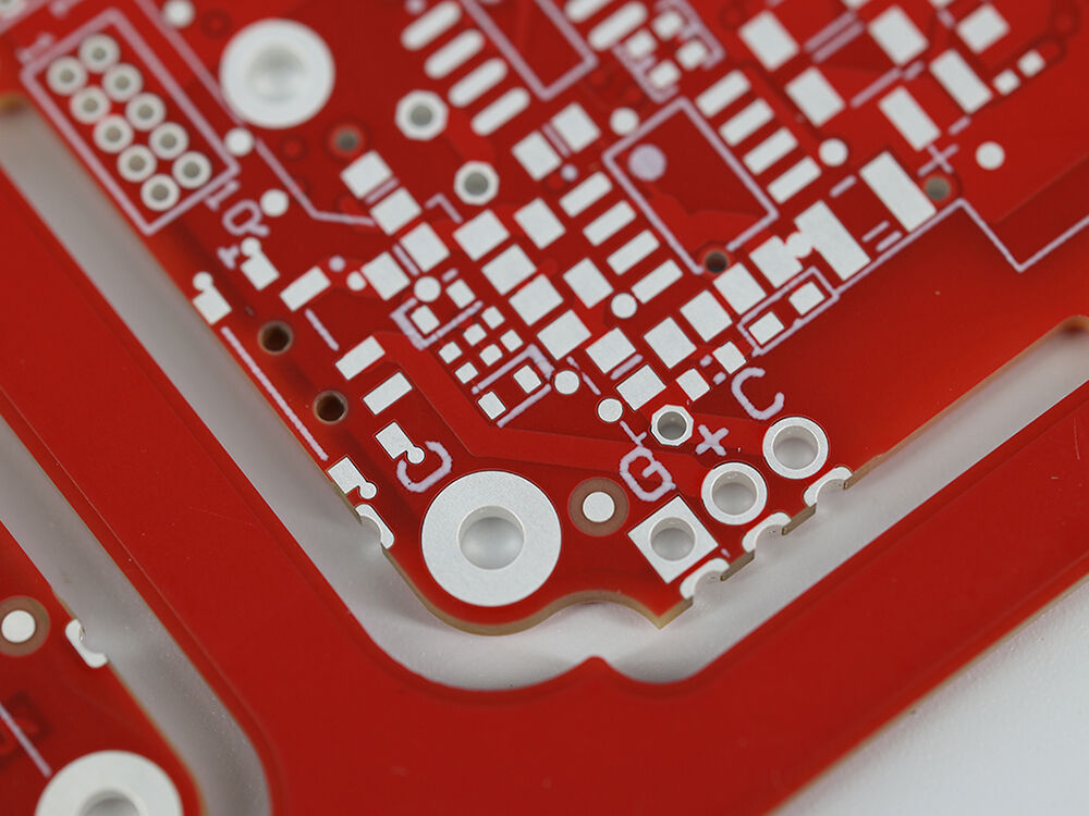
Bare board PCBs form the critical foundation of every electronic device. These unpopulated printed circuit boards provide the electrical pathways and mechanical support enabling complex circuits and devices to function. As manufacturing continues to advance in complexity—especially with multilayer and high-density PCBs—the importance of rigorous quality control and testing in bare board manufacturing becomes paramount.
Defects introduced during fabrication, such as opens, shorts, misregistration, and contamination, can significantly impair product performance or cause complete failure post-assembly. Such failures result in costly rework, warranty claims, and reputational damage. For manufacturers and design engineers alike, understanding and implementing comprehensive PCB inspection and bare PCB testing protocols ensures compliance with critical standards, reduces production risks, and improves overall PCB manufacturing quality.
This article explores the essential quality assurance steps and testing techniques used in modern PCB fabrication. We will delve into critical inspection processes, from incoming materials to electrical testing methods like continuity and isolation tests, and automated systems such as AOI (Automated Optical Inspection) and flying probe testing. Additionally, we highlight how industry standards (IPC-600, IPC-6012) guide manufacturers in delivering reliable bare boards ready for assembly.
Key Takeaways from this Section:
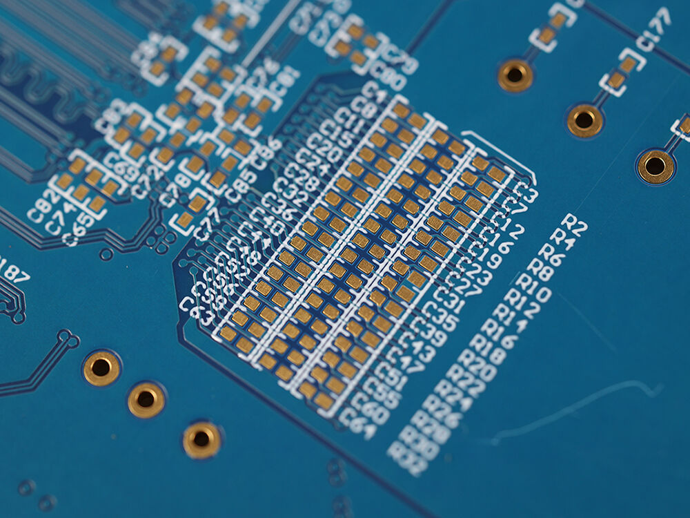
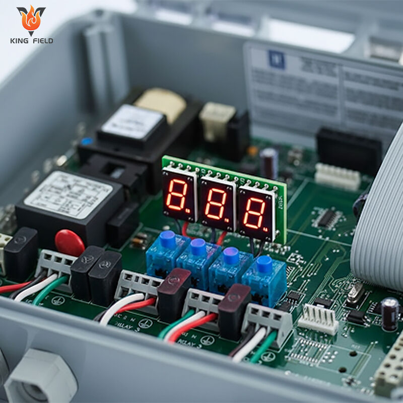
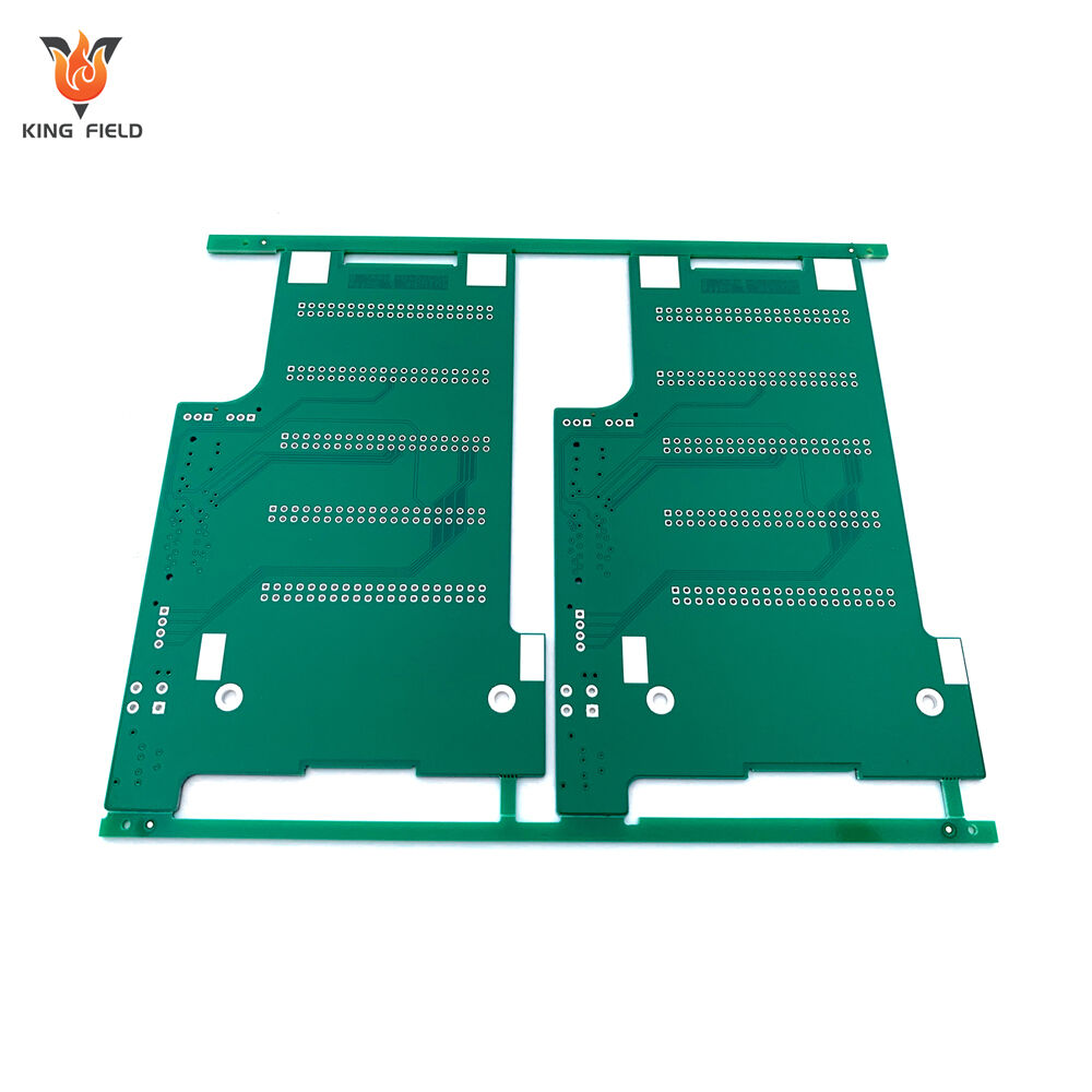
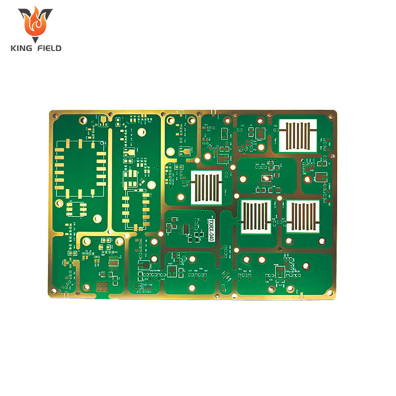
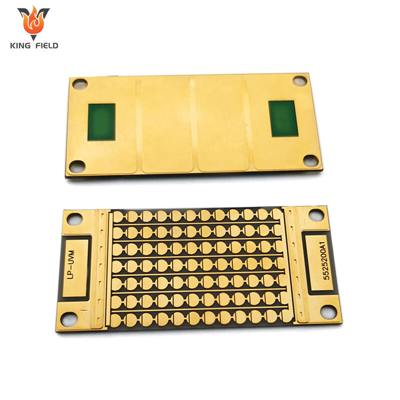
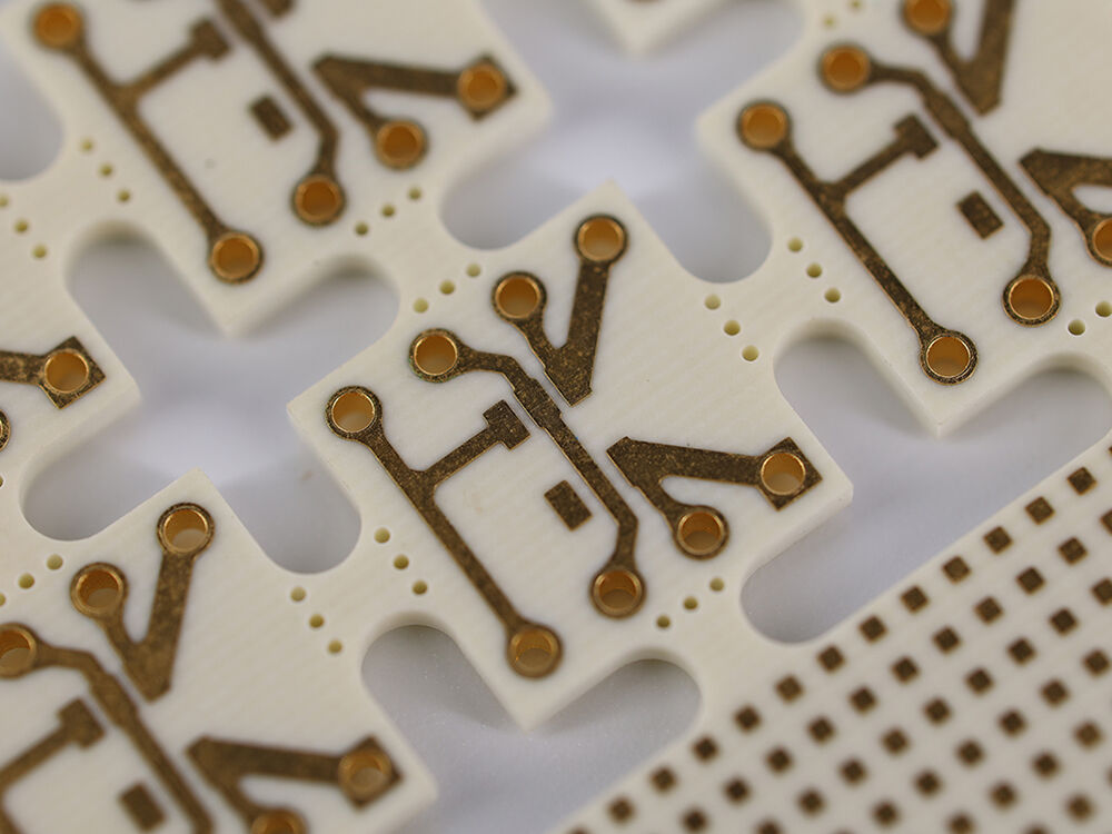
A bare board PCB, also known simply as an unpopulated PCB, is the foundational printed circuit board prior to any component assembly. It consists of several key elements designed to facilitate electrical interconnections and mechanical support once electronic components are installed.
The bare board serves as the electrical backbone of the circuit, supporting both the physical placement of components and their electrical interconnectivity. Its quality directly affects the downstream PCB assembly process and the overall device reliability.
Bare PCBs come in a wide range of types depending on complexity and application:
|
Question |
Brief Answer |
|
What exactly is included in a bare board? |
Copper layers, dielectric substrates, solder mask, and surface finish. No components. |
|
How does a bare board differ from a PCBA? |
A PCBA is an assembled board with components soldered onto the bare PCB. |
|
What are typical surface finishes on bare boards? |
ENIG, HASL (lead-free or leaded), OSP, Immersion Silver, and others. |
|
How do multilayer boards improve PCB functionality? |
By enabling more signal layers, internal ground and power planes, and complex impedance control. |
A consumer electronics company faced frequent field failures traced back to intermittent opens on their rigid-flex bare boards. After implementing tighter PCB quality control and adopting more rigorous bare board testing including microsection analysis, the incidence of failures reduced by 78%, directly improving customer satisfaction and reducing warranty costs.
Summary: Understanding what constitutes a bare board PCB and its critical role in device architecture sets the stage for grasping why strict PCB manufacturing quality control and testing processes are essential to avoid expensive failures downstream.
In the complex process of printed circuit board fabrication, ensuring the highest quality in your bare board PCBs is paramount. Each manufacturing step—from laminating layers to surface finishing—introduces potential pitfalls that can manifest as defects impacting electrical performance and mechanical integrity. Without rigorous quality control in PCB manufacturing, these defects risk propagating into costly assembly errors and product failures.
|
Fabrication Step |
Typical Defects Introduced |
|
Laminating |
Delamination, voids, uneven bonding |
|
Drilling |
Misaligned or oversized holes, burrs |
|
Plating |
Incomplete or uneven plating, voids, insufficient thickness |
|
Imaging & Etching |
Trace width variation, under-etching/over-etching, opens/shorts |
|
Solder Mask Application |
Incomplete coverage, bridging, peel-off |
|
Surface Finishing |
Contamination, oxidation, poor adhesion |
Each defect can drastically affect the bare board's electrical continuity, signal integrity, and mechanical strength—elements fundamental to overall PCB reliability and product success.
“A rigorous quality control regimen is non-negotiable in bare board manufacturing. The costs of undetected defects far outweigh investment in comprehensive inspection and testing.” — Senior Quality Engineer, Shenzhen PCB Manufacturer
Defects not detected during bare board manufacturing can manifest in the following ways:
|
Defect Type |
Impact if Undetected |
Detection Methods |
|
Opens/Breaks |
Open circuits, device malfunction |
Continuity Testing, AOI, Flying Probe |
|
Shorts |
Short circuits, device failure |
Isolation Testing, AOI, Flying Probe |
|
Misregistration |
Misaligned layers cause shorts/opens |
Imaging Inspection, AOI |
|
Surface Contamination |
Solderability reduction, intermittent connections |
Visual, AOI, Surface Finish Inspection |
|
Copper Peel |
Trace loss under stress or heat |
Microsection Analysis |
|
Voids/Delamination |
Mechanical failure, signal issues |
Microsection, X-ray Inspection |
|
Warpage |
Assembly misalignment or stress failure |
Visual Inspection, Measurement Tools |
To guarantee the highest bare board testing quality and minimize PCB manufacturing defects, manufacturers employ a robust set of quality control (QC) processes throughout production. These six key QC stages provide early detection of issues, ensuring the bare board PCB meets design specs and reliability standards before moving downstream.
Purpose: Ensure raw materials meet required standards before fabrication begins.
Purpose: Continuous monitoring during production to catch and rectify defects quickly.
Purpose: Validate that the electrical paths are correctly formed, and no unintended connections exist.
Test Methods:
Flying Probe Test:
Bed-of-Nails Test:
Purpose: Detects surface and geometric defects using advanced image processing.
AOI combines the speed of automation with high sensitivity, catching defects challenging for manual inspection.
Purpose: Microscopic examination of the internal structure of PCBs.
Purpose: Validate surface finish properties critical to solderability and long-term reliability.
|
QC Process |
Primary Focus |
Importance for PCB Manufacturing Quality |
|
Incoming Material Inspection |
Verify raw materials spec and quality |
Prevents upstream defects from material faults |
|
In-Process Inspection |
Early defect detection in fabrication |
Reduces scrap and rework, improves process control |
|
Electrical Testing (Continuity & Isolation) |
Ensures correct electrical connectivity |
Validates electrical functionality before assembly |
|
Automated Optical Inspection (AOI) |
Detects surface defects and dimensional variances |
Rapid, automated, and high coverage quality check |
|
Microsection Analysis |
Detect internal structural defects |
Essential for multilayer and high-reliability PCBs |
|
Surface Finish Inspection |
Check solderability and finish quality |
Critical for reliable solder joints and long-term durability |
“Integrating these six quality control processes into the PCB manufacturing workflow substantially improves yield and product reliability, ultimately saving time and cost downstream.” — Quality Manager, Leading PCB Fabricator
In bare board PCB manufacturing, identifying and addressing defects early via rigorous testing and inspection is crucial. These defects can range from minor cosmetic issues to critical faults that impair electrical continuity or mechanical integrity, dramatically affecting downstream assembly and product reliability.
Opens (Open Circuits) These are unintended breaks in conductive paths or copper traces that disrupt signal or power flow. Opens often result from incomplete etching, plating failures, or physical damage during handling.
Shorts (Short Circuits) Unintended electrical connections between adjacent traces or pads caused by over-etching, solder mask bridging, or residue. Shorts can cause immediate malfunction or permanent damage.
Misregistration Occurs when the copper layers, solder mask, or silkscreen are not properly aligned with each other or with drill holes, causing connectivity errors or soldering issues.
Surface Contamination and Oxidation Presence of dirt, oils, or oxidation layers on copper or pads reduces solderability and leads to weak or unreliable solder joints.
Copper Peel or Delamination Separation or peeling between copper layers and dielectric substrates undermines electrical integrity and mechanical strength.
Voids and Blisters Internal voids in laminates or blistering on the board surface can cause mechanical weakness or electrical failures, often detected in microsection analysis.
Trace Breakage and Missing Copper Broken or incomplete copper traces may result from tooling errors or excessive mechanical stress during fabrication or depanelization.
Warpage and Bowing Excessive bending or distortion of the PCB affects assembly alignment and can cause solder joint failures or mechanical stresses in final products.
|
Defect Type |
Impact on PCB Performance |
Typical Detection Method |
|
Opens |
Signal interruptions, device failure |
Continuity testing, AOI, Flying probe |
|
Shorts |
Short circuits causing malfunction or damage |
Isolation testing, AOI, Flying probe |
|
Misregistration |
Poor soldering, intermittent electrical contact |
Visual inspection, AOI |
|
Surface Contamination |
Reduced solder joint strength; poor assembly yield |
AOI, Surface Finish Inspection |
|
Copper Peel/Delamination |
Loss of electrical path, mechanical failure |
Microsection analysis, X-ray |
|
Voids/Blisters |
Reduced insulation and mechanical strength |
Microsection, X-ray |
|
Trace Breakage |
Intermittent/open circuits |
Continuity testing, AOI |
|
Warpage |
Assembly problems, alignment errors |
Visual inspection, specialized measuring |
Detecting these defects before assembly saves time, resources, and capital. Bare board issues are notably more difficult and costly to address after component mounting. Conversely, thorough bare PCB testing and inspection during fabrication helps:
A manufacturer producing high-speed multilayer PCBs experienced frequent open circuits due to micro-etch faults. By integrating Automated Optical Inspection immediately after etching and complementing it with flying probe testing for electrical validation, defect rates declined by 65%, boosting throughput and customer satisfaction.
In maintaining consistent PCB manufacturing quality, adherence to well-established industry standards is essential. These standards provide frameworks to define acceptability criteria, testing requirements, and performance specifications tailored to various application demands—from consumer electronics to mission-critical aerospace systems.
|
IPC Class |
Application Type |
Quality & Reliability Requirements |
|
Class 1 |
General Electronics (Consumer) |
Basic functionality; lenient defect tolerances |
|
Class 2 |
Dedicated Service Electronics (Industrial) |
Higher reliability; moderate inspection rigor |
|
Class 3 |
High-Reliability Electronics (Medical, Aerospace, Telecom) |
Stringent inspections and testing; high reliability |
Choosing the correct IPC class dramatically influences manufacturing rigor and cost:
|
Standard |
Scope |
Application |
|
IPC-600 |
Visual acceptability criteria |
All PCB bare board inspections |
|
IPC-6012 |
Performance & qualification |
Critical for high-reliability board applications |
|
RoHS |
Environmental compliance |
Materials and chemical substances |
|
UL |
Safety & flammability |
Material safety and electrical insulation |
|
ISO 9001, ISO13485 |
Quality management systems |
Manufacturer process consistency and traceability |
"Adhering to IPC standards ensures not only the PCB manufacturing quality but also peace of mind that boards will perform reliably in demanding environments. It’s the benchmark between a good board and a great one." — Ross Feng, Industry Expert and CEO of Viasion Technology
Ensuring exceptional quality control and testing in bare board manufacturing is fundamental to delivering bare board PCBs that meet or exceed industry expectations for reliability, performance, and durability. As the backbone of every electronic assembly, the bare PCB must be free from defects like opens, shorts, misregistration, and contamination that can compromise the entire product lifecycle.
Through a combination of rigorous incoming material inspections, continuous in-process monitoring, precise electrical testing (including continuity and isolation tests), advanced automated optical inspections (AOI), and in-depth microsection analysis, manufacturers effectively identify and mitigate potential quality issues before assembly. Validating surface finish quality further ensures solderability and long-term operational integrity.
Adhering to recognized standards such as IPC-600 and IPC-6012 is critical to establishing acceptance criteria and performance benchmarks tailored to the needs of consumer electronics, industrial applications, or high-reliability sectors like aerospace and medical devices. This disciplined approach not only reduces costly scrap and rework but also accelerates production timelines and enhances customer trust.
“In the world of electronics manufacturing, quality is not just a checkbox—it is the difference between products that succeed and those that fail in the field. Investing in comprehensive bare board testing and stringent PCB quality control processes delivers sustainable value and superior reliability.” — Ross Feng, PCB Industry Veteran and CEO of Viasion Technology
By integrating these proven PCB quality assurance (QA) methodologies and selecting trusted manufacturers committed to best practices, engineers and procurement teams can confidently reduce risks and elevate product quality from the very foundation up.
 Hot News
2026-01-17
2026-01-16
2026-01-15
2026-01-14
2026-01-13
2026-01-12
2026-01-09
2026-01-08