Meta Title: PCB Assembly for Wearable Devices — Flexible PCB Materials, SMT Techniques & DFM Meta Description: Learn best practices for wearable PCB assembly: flexible PCB materials (polyimide, coverlay), SMT/reflow profiles, conformal coating, RF tuning, DFM guidelines, and common failure prevention.
1. Introduction: The Revolution of Flex and Rigid-Flex PCBs
The past decade has marked a groundbreaking shift in the way electronic devices are designed, especially in the realm of wearable technology and medical devices. Today’s consumers expect not just smart features, but ultra-compact, featherweight, and robust gadgets like smartwatches, fitness trackers, hearing aids, biosensor patches, and more. These demands have driven wearable PCB assembly into the spotlight, forcing designers and manufacturers to rethink everything from materials to connection strategies.
Flexible PCB (FPC) and rigid-flex PCB technologies have become the backbone of this new wave. Unlike traditional PCBs, flexible printed circuit boards bend, twist, and conform to tiny, oddly shaped product enclosures. Rigid-flex PCBs go further, integrating both bendable and stiff regions within the same board, creating seamless electrical connections in products’s toughest corners. These innovations in FPC assembly not only reduce size and weight but improve device durability, enhance performance, and enable the new possibilities like curved screen designs or medical sensors that fit comfortably against the body.
According to a 2025 industry survey (IPC, FlexTech), over 75% of new wearable electronics and medical device designs now feature some form of flex circuit or rigid-flex integration. This trend is set to accelerate as products get smarter, thinner, and more resilient. In fact, high-density interconnects (HDI), ultra-small 0201 SMT components, and advanced polyimide flexible PCB materials have become standard in PCB assembly for wearable devices.
“The heart of wearable innovation is miniaturization. But miniaturization is only possible thanks to breakthroughs in flexible circuit board manufacturing and assembly.” — Paul Tome, Product Manager Flex & Rigid-Flex, Epec Engineered Technologies
Here’s what makes this new era of wearable electronics PCB so exciting:
- Space & Weight Savings: Modern wearables can be as thin as a coin yet offer full connectivity, thanks to their flexible PCB stack-ups and miniaturized components.
- Durability & Comfort: Polyimide FPCs can reliably withstand thousands of bend cycles, making them perfect for wristbands, patches, and headbands that must move with the wearer.
- Power & Performance: Efficient layouts, precise routing, and advanced assembly, including optimized SMT soldering and conformal coating for PCBs, help manage power loss and electromagnetic interference (EMI/RF).
- Speed to Innovation: DFM for flexible PCBs and rapid prototyping techniques (like 3D-printed flex circuits) allow companies to quickly iterate and bring new ideas to market.
Table 1: Comparison of PCB Technologies in Wearable Devices
|
Feature
|
Rigid PCB
|
Flexible PCB (FPC)
|
Rigid-Flex PCB
|
|
Shape Flexibility
|
None
|
High (bends, twists)
|
High (integrated bends/zones)
|
|
Miniaturization
|
Limited
|
Excellent
|
Excellent
|
|
Weight
|
Heavy
|
Ultra-light
|
Light
|
|
Durability
|
Moderate
|
High (with proper design)
|
Very High
|
|
Assembly Complexity
|
Standard SMT
|
Requires special SMT/DFM
|
Highest, needs hybrid tech
|
|
Use Case
|
Rigid devices
|
Fitness/smart bands, patches
|
Smartwatches, implants, med
|
As we dive deep into this guide, you’ll learn not just the “what” but the “how” behind next-gen wearable PCB assembly—from choosing the right flex PCB materials and mastering SMT for flexible PCBs to overcoming real-world assembly and reliability challenges. Whether you’re an engineer, designer, or supply chain manager in the IoT, health tech, or consumer electronics sectors, these insights will help you deliver better, smarter devices.
2. What Are Flexible and Rigid-Flex PCBs?
In the field of wearable electronics PCB design, not all printed circuit boards are created equal. Flexible PCBs (FPCs) and rigid-flex PCBs have emerged as the gold standard for modern wearables, IoT modules, and medical devices, where durability, space-efficiency, and unique form factors are paramount. Let’s explore what sets these advanced PCB technologies apart—and how they unlock innovation in products like smartwatches, fitness trackers, and biosensor patches.
Flexible Printed Circuit Boards (FPCs)
A flexible printed circuit board is built using a thin, bendable substrate—typically a polyimide (PI) film—that can flex, fold, and twist without breaking. Unlike traditional rigid boards based on FR-4, FPCs are purpose-built to conform to the dynamic, compact environments of wearable devices.
Typical stack-up for flexible PCBs:
|
Layer
|
Material
|
Typical Thickness
|
Function
|
|
Top Overlay
|
Polyimide Coverlay
|
12–25 µm
|
Surface protection, insulation
|
|
Copper Foil
|
Copper
|
12–35 µm
|
Conductive signal/power layer
|
|
Substrate
|
Polyimide Film (PI)
|
12–50 µm
|
Flexible structure
|
|
Copper Foil
|
Copper (optional)
|
12–35 µm
|
For double-sided/multilayer
|
|
Bottom Overlay
|
Polyimide Coverlay
|
12–25 µm
|
Surface protection, insulation
|
Key facts:
- Bend radius: For robust designs, the minimum bend radius should be at least 10× total board thickness.
- Trace width/spacing: Often as fine as 0.05–0.1 mm spacing on advanced boards.
- Copper foil thickness: Commonly found in 12–70 µm range, with thinner foils enabling tighter bends.
- Coverlay film: Provides both mechanical protection and electrical insulation.
FPC Assembly supports both single-layer and complex multilayer builds, and enables designers to create device enclosures as thin as 0.2 mm—perfect for next-gen fitness trackers or smart patches.
Rigid-Flex PCBs
A rigid-flex PCB combines the best of both worlds: sections of the circuit board are built as hard, durable rigid boards for mounting delicate SMT components, while other areas are left flexible to facilitate bending or folding. These flexible and rigid regions are seamlessly integrated through precise fabrication processes, reducing assembly complexity and the need for bulky connectors.
Typical structure of a rigid-flex PCB:
- Rigid sections: Standard FR-4 (or similar) with copper layers, used for component mounting.
- Flex sections: Polyimide-based FPC layers connecting rigid sections, allowing for dynamic motion and compact stacking.
- Interlayer connection: Microvias or through vias, often implemented for HDI (High-Density Interconnect) design, support multi-layer signal paths and power delivery.
- Transition zones: Carefully designed to avoid stress and crack propagation.
Advantages in wearable devices:
- Maximum design freedom: Enables device designs that would be impossible with rigid-only PCBs.
- Fewer connectors/interconnects: Reduces overall weight, thickness, and failure points.
- Superior reliability: Critical for high-reliability applications (e.g., medical implants, military-grade wearables).
- Enhanced EMI and RF shielding: Through layered ground planes and closer control of impedance.
Real-World Applications in Wearables and Medical Devices
Smartwatches:
- Use multi-layer flexible PCB stack-up for signal routing, touchscreens, display drivers, and wireless modules around curved watch housings.
- Flexible antennas and battery connections benefit from FPC assembly to maintain device integrity during wrist flexion.
Fitness Trackers and Biosensor Patches:
- Polyimide flexible PCBs with fine-pitch SMT components enable disposable or semi-disposable, ultra-thin form factors (<0.5 mm).
- Embedded sensors (like accelerometers, heart rate, or SpO₂ LEDs) directly on FPCs improve signal quality and product comfort.
Medical Devices:
- Rigid-flex PCBs power implantable monitors and patient wearables by combining reliability, low weight, and resistance to repeated flex cycling—often exceeding 10,000 cycles in flex testing.
Case Study: A leading fitness tracker manufacturer leveraged 6-layer FPCBs with 0.05 mm traces and 0201 components, achieving a final board assembly thickness of 0.23 mm. This allowed for a sub-5 gram device featuring continuous ECG and motion tracking – something simply unattainable with classic rigid PCBs.
Terminology Quick Reference
|
Term
|
Also Known As
|
Typical Use
|
|
FPC/FPCB
|
Flex PCB/Flex Circuit
|
Wearable/curved electronics
|
|
PI film
|
Polyimide
|
Substrate in flexible PCBs
|
|
Coverlay
|
Cover film
|
Protective layer in FPC stacks
|
|
Rigid-flex PCB
|
Hybrid PCB
|
Smartwatches, implants
|
|
Microvias
|
Laser-drilled vias
|
HDI signal/power interconnects
|
In summary: Flexible and rigid-flex PCBs are not just alternatives to rigid boards—they’re the very engines that power the next generation of smarter, smaller wearable and medical devices. Understanding the materials, structures, and core concepts behind them underpins every other design and assembly decision in wearable PCB assembly.
Ready for Section 3? Type 'Next' and I’ll continue with “Advantages of Flexible PCBs for Wearables and Medical Devices”—including lists, deep-dive explanations, and actionable industry knowledge.

3. Advantages of Flexible PCBs for Wearables and Medical Devices
When engineering advanced wearable electronics PCB solutions or creating compact medical devices, flexible PCBs (FPCs) are the foundation for both innovation and function. Their unique properties drive miniaturization, improve reliability, and enable features that reshape what’s possible in consumer and healthcare technology.
Miniaturization and Space Savings: Unlocking New Designs
One of the most outstanding benefits of a flexible printed circuit board is its exceptional thinness and conformability. Unlike conventional rigid boards, FPCs can be as thin as 0.1–0.2 mm, with stack-ups built for both single and multilayer configurations. This enables designers to route critical signals and power in tight, curved, or layered spaces within the smallest of wearable devices.
Example Table: Flexible PCB Thickness by Application
|
Device Type
|
FPC Layer Count
|
Typical PCB Thickness (mm)
|
Example Component Density
|
|
Fitness Tracker
|
1–2
|
0.10–0.25
|
0201 SMT, microcontrollers
|
|
Smartwatch
|
2–4
|
0.13–0.35
|
RF/antenna, dense sensors
|
|
Biosensor Patch
|
1–2
|
<0.20
|
Thin flex, wireless module
|
|
Hearing Aid
|
2–3
|
0.15–0.28
|
High-density sound processor
|
Key fact: A flexible PCB can often replace several rigid boards and their interconnects, reducing weight by up to 80% and volume by as much as 70% versus traditional PCB for wearables approaches.
Durability and Reliability Under Repeated Bending
Polyimide-based FPCs are engineered to withstand thousands, even tens of thousands of bends, twists, and flex cycles. This is vital for wearables, which are routinely subjected to wrist, ankle, or body movement and must operate flawlessly for years.
- Flex-cycle testing: Leading manufacturers test their wearable PCB assemblies to standards exceeding 10,000 flex cycles without structural or electrical failure.
- Delamination resistance: The combination of copper foil and strong adhesives in the FPC stack-up minimizes layer separation, even under physical stress.
- Avoidance of solder cracking: Strategic placement of SMT components, and the use of underfill in stress zones, prevents fatigue failures that are common in rigid boards.
Quote:
“Without flex PCB durability, most smart health and fitness wearables would fail after just a few days or weeks of real-world use. Robust FPC assemblies are now the industry baseline.” — Lead Engineer, Global Fitness Device Brand
Fewer Interconnects, Higher System Reliability
Traditional PCB assemblies—especially in 3D, folded device layouts—require connectors, jumpers, and soldered cables. Each interconnect is a potential failure point. Flexible PCB assembly allows multiple circuit segments to be integrated into a single structure, decreasing the number of:
- Solder joints
- Wire harnesses
- Mechanical connectors
This results in:
- Greater shock/vibration resistance (crucial for active lifestyle wearables)
- Simpler assembly processes
- Fewer warranty issues due to connector/cable faults
Fact: A typical fitness tracker using a single FPC can reduce its interconnect count from 10+ down to 2 or 3, while at the same time cutting assembly time by more than 30%.
Design Freedom: Complex Shapes and Layering
The “bend-and-stay” capability of modern polyimide flexible PCBs enables new levels of design freedom:
- Wrapping circuitry around curved batteries or display modules.
- Stacking multiple electronics layers for high-density interconnect (HDI) PCBs.
- Creating “origami” assemblies that fold to fit inside biomimetic or non-rectangular enclosures.
List: Design Features Enabled By Flexible PCB
- Wearable patches (medical electrodes, continuous glucose monitoring): Ultra-thin, drapes over skin
- AR/VR headbands or eyewear: Conforms to facial shape, enhances comfort
- Smart rings/bracelets: Encircles small radii without cracking or failing
- Bio-integrated electronics: Folds or flexes with soft human tissue
Reduced Cost in Mass Production
While initial tooling for flex circuits may be higher, this is offset by:
- Lower component count (connector/cable elimination)
- Shorter SMT assembly lines (less manual labor)
- Improved yield with fewer interconnect-related defects
Over high volumes seen in consumer wearables and medical patches, the total cost of ownership trends lower than rigid assemblies, especially when accounting for warranty returns or post-sale failures.
4. Advantages of Rigid-Flex PCBs
In the journey of wearable PCB assembly and advanced electronics for portable devices, the engineering community has discovered the power of combining both worlds—rigid and flexible PCBs—to create unmatched products. Rigid-flex PCBs have carved out an essential role in medical technology, military-grade equipment, AR/VR devices, and high-end consumer wearables by offering the perfect blend of durability, versatility, and performance.
What Is a Rigid-Flex PCB?
A rigid-flex PCB is a hybrid structure that integrates layers of rigid (FR-4 or similar) printed circuit boards with layers of flexible circuits (FPCs), typically made from polyimide. The flexible sections connect rigid regions, enabling 3D folding, use in uniquely shaped enclosures, and direct integration into moving parts like wristbands or headgear.
Key Benefits of Rigid-Flex PCB Technology
1. Superior Structural Reliability
Rigid-flex PCBs greatly reduce the need for connectors, jumper wires, crimps, and solder joints. This is vital in wearable electronics PCB assemblies, which are exposed to frequent bending, drops, and vibration.
- Reduced interconnect points: Each eliminated connector reduces a potential failure hotspot, lowering the overall risk of device failure.
- Enhanced shock/vibration resistance: Integrated structures withstand mechanical abuse better than assemblies with connectors and wiring harnesses.
- Better suited for high-reliability and mission-critical wearables, such as implantable medical devices or military communication units, where a single point of failure is unacceptable.
2. Compact and Lightweight Packaging
Because the rigid and flexible sections are seamlessly integrated, rigid-flex PCBs dramatically reduce overall device thickness and weight. This is essential for smartwatches, wireless earbuds, and compact medical monitors.
- Integrated circuits and fewer cables allow for innovative, miniaturized packaging that can conform to organic shapes.
- Weight reduction: Flex areas typically add only 10–15% of the combined size and weight compared to separate rigid PCBs with cable assemblies.
- Space savings: Rigid-flex solutions often reduce circuit volume by 30–60%, and allow for true 3D packaging architectures (folded, stacked, or curved assemblies).
3. Enhanced Electrical Performance
High-speed signals and RF traces benefit from rigid area’s controlled dielectric properties and ground shielding, while flex regions manage interconnections in tight spaces.
- Controlled impedance: Excellent for high-frequency circuits (Bluetooth, Wi-Fi, medical telemetry).
- Improved EMI/RF shielding: Layered stack-up and ground isolation enable better compliance with EMC standards.
- Signal integrity: Microvias and HDI routing ensure signal paths are short, direct, and optimized for low noise.
Table: Key Capabilities Unlocked by Rigid-Flex PCBs
|
Feature
|
Benefit
|
Example Use Case
|
|
Fewer connectors/interlinks
|
Lower failure risk, easier troubleshooting
|
Medical implant, military wearable
|
|
3D foldable design
|
Fits curved or stacked cases
|
Smartwatches, AR/VR goggles
|
|
Enhanced shielding/grounding
|
RF/EMI integrity
|
Biosensors, wireless headsets
|
|
Integrated assembly zones
|
Streamlined mass production
|
Health patches, patient monitors
|
4. Streamlined PCB Assembly and Reduced Cost (Long-Term)
While the upfront PCB cost for rigid-flex is higher than simple FPC or rigid only, the long-term savings are substantial:
- Simplified assembly: Single, integrated board means fewer parts, steps, and potential errors.
- Faster automated assembly: SMT and THT lines run smoother with fewer separate PCBs and connectors to align.
- Cost-effective over volume: Reducing post-sale repairs, returns, or assembly rework costs pays dividends for devices with lifespans of several years.
5. Withstanding Harsh Environments
Rigid-flex PCBs are ideal for use in hostile medical or outdoor environments:
- High temperature tolerance: Polyimide flex and high-Tg rigid sections withstand up to 200°C (short duration), supporting sterilization or outdoor deployment.
- Corrosion, chemical, and UV resistance: Essential for devices in contact with sweat, cleaning solutions, or sunlight.
- Moisture protection: Enhanced with conformal coating for PCBs and parylene/silicone encapsulation in flex zones.
6. Design Freedom for Inventive Applications
Rigid-flex circuits allow new geometry:
- Wearable cameras—PCB can coil around batteries and sensors
- Neural monitoring headbands—PCB follows head contours without exposed wires
- Medical patches for infants—Thin, foldable, yet robust—allows continuous monitoring without causing skin damage
Why Rigid-Flex Stands Out for the Future
The fusion of rigidity and flexibility in a single PCB unlocks a new world of wearable possibilities, giving designers a robust canvas for smart, connected medical tech, next-generation fitness trackers, AR/VR wearables, and beyond.
5. Key Design Challenges in Wearable PCB Assembly
The innovation and miniaturization benefits of wearable PCB assembly are tremendous, yet they bring unique and complex design challenges that engineers must address to ensure reliability, durability, and optimal user experience. These challenges stem directly from the demands of flexible PCB and rigid-flex PCB technologies, as well as the ever-decreasing size and ever-increasing expectations of today’s wearable electronics.
Miniaturization and High-Density Interconnects (HDI)
Miniaturization is at the very heart of designing circuits for wearables. Devices like smartwatches and health patches require PCBs as thin as a few tenths of a millimeter, with ever-increasing numbers of functions packed into every square millimeter.
- HDI technology: Utilizes microvias (as small as 0.1 mm), ultra-fine traces (≤0.05 mm), and stacked layer constructions to enable highly dense routing.
- Component size: 0201 SMT components are commonly used in flex PCB assembly for wearables, putting immense pressure on pick-and-place accuracy (<0.01 mm) and soldering precision.
- Spacing constraints: Signal integrity, power routing, and thermal management must all be maintained in a footprint that may be 15×15 mm or less.
Table: HDI and Miniaturization in Wearable PCB Assembly
|
Parameter
|
HDI/Flex Standard (Wearable)
|
Typical Rigid PCB (Legacy)
|
|
Via diameter
|
0.1 – 0.15 mm (microvia)
|
0.25 – 0.5 mm
|
|
Trace width
|
0.05 – 0.10 mm
|
0.15 – 0.25 mm
|
|
SMT component size
|
0201, 0.4 mm pitch BGA
|
0402 – 0603, ≥0.8 mm BGA
|
|
Board thickness
|
0.13 – 0.3 mm (flex zone)
|
1.0 – 2.0 mm (rigid only)
|
Flexibility: Material Stress, Bend Radius, and Placement Constraints
Wearable devices require board regions that flex with movement—potentially thousands of times a day. Designing for flexibility means understanding stress concentration, ensuring the minimum bend radius (≥10× total thickness), and optimizing layer stacks to withstand repeated deformation without performance loss.
- Polyimide flexible PCB layers are chosen for their fatigue resistance, but improper layout or stack-up can still cause cracking or delamination.
-
Placement guidelines:
- Heavy or tall components must be located on rigid or low-stress zones.
- Traces should be routed along the neutral axis of bends and avoid via clusters or sharp corners.
-
Routing best practices:
- Use curved traces, not sharp angles.
- Maintain wider trace spacing where possible.
- Avoid vias in areas subject to frequent flexing.
Power Efficiency and Battery Constraints
Most wearables are battery-powered and must operate for days—or even weeks—on a single charge. Power management on flexible printed circuit boards is a balancing act between space, trace resistance, thermal effects, and overall system efficiency.
- Low-power microcontrollers, Bluetooth modules, and power management ICs are standard.
-
Power delivery:
- Use wide power traces and solid ground planes for lowest possible resistance.
- Careful decoupling placement to limit voltage drops and prevent oscillations.
- Stack-up and routing should minimize IR loss and cross-talk at high density.
Moisture Resistance and Environmental Robustness
Wearables are exposed to sweat, skin oils, and the elements, raising the bar on conformal coating for PCBs, encapsulation, and assembly cleanliness.
-
Conformal coating types:
- Parylene: Thin, pinhole-free; excellent for medical and high-reliability applications.
- Acrylic, Silicone: More cost-effective, good moisture and chemical resistance.
- Selective coating: Applied only where needed to save weight, cost, and production time.
-
Testing for robustness:
- Devices must pass high humidity, corrosion, and “water splash” tests simulating months of continuous wear.
RF/EMI Stability
Advanced PCB assembly for wearable devices often incorporates wireless radios (Bluetooth, NFC, Wi-Fi, Zigbee). Ensuring clean signal transmission requires attention to RF design and EMI shielding in extremely compact spaces:
-
Impedance control:
- 50 Ω traces, via fences, consistent copper balancing.
- Use of a controlled impedance calculator for critical antennas and RF traces.
- RF/digital isolation: Place RF modules and digital logic in dedicated board zones, add local ground shields, and use isolation gaps.
Rigid FR-4 vs. Flexible Polyimide (FPC) Comparison
|
Attribute
|
Rigid FR-4 PCB
|
Flexible Polyimide FPC
|
|
Bendability
|
None
|
Excellent
|
|
Minimum thickness
|
~0.8 mm
|
~0.1 mm
|
|
Flexural cycles
|
Fails after 10s-100s
|
>10,000
|
|
Weight
|
High
|
Ultra-light
|
|
Environmental sealing
|
Optional conformal
|
Generally required
|
|
Cost per in²
|
Low (high volume)
|
Higher, but offset by less material/connectors
|
Summary Checklist for Success in Wearable PCB Assembly
- HDI design with microvias and fine traces
- Maintain bend radius ≥10× stack thickness
- Keep sensitive/large parts off flex zones
- Route traces along neutral axis and avoid stress concentrators
- Plan for moisture/environmental protection
- Design for RF and EMI/ESD reliability from the outset
Successfully overcoming these challenges is essential for delivering durable, miniaturized, and reliable wearable electronics PCB products. Every choice, from stack-up and materials to SMT assembly techniques and environmental protection, influences real-world robustness and consumer satisfaction.
6. Materials and Stack-Up Design for Flexible and Rigid-Flex PCBs
Modern wearable PCB assembly relies heavily on material science and precise stack-up engineering. The selection of flexible PCB materials, copper weights, adhesives, coverlay, and more directly impacts the performance, reliability, and manufacturability of both flexible printed circuit boards (FPCs) and rigid-flex PCBs. Choosing the right materials and stack-up arrangement ensures your wearable device delivers on size, weight, flexibility, and lifetime—even under constant physical stress.
Core Materials for Flexible and Rigid-Flex PCBs
Polyimide (PI) Film
- Gold standard substrate for flexible and rigid-flex PCBs.
- Offers excellent mechanical flexibility, high heat resistance (up to 250°C), and superb chemical stability.
- Thin gauges, typically 12–50 µm, cater to both ultra-thin wearable patches and more robust flex sections.
Copper Foil
-
Signal & power layer: Commonly available in 12–70 µm thickness.
- 12–18 µm: Enables ultra-tight bends, used in high-density flex regions.
- 35–70 µm: Supports higher currents for power or ground planes.
- Rolled annealed copper is preferred for dynamic flexing due to its superior fatigue resistance, while electro-deposited copper is sometimes used for less demanding, mostly static applications.
Adhesive Systems
- Join layers together (PI and copper, coverlay and copper, etc.).
- Acrylic and epoxy adhesives are popular, but for high-reliability/medical FPCs, adhesiveless processes (directly laminating copper onto PI) reduce failure risk and improve thermal endurance.
Coverlay/Cover Film
- Polyimide-based coverlay films of 12–25 µm thickness act as protective and insulating layers over the circuit, especially critical in sweat-exposed or mechanically stressed wearables.
- Protects the circuitry from abrasion, moisture, and chemical ingress while maintaining flexibility.
Rigid Section Materials (Rigid-Flex)
- FR-4 (fiberglass/epoxy): Standard for the rigid portions, offering component stability, strength, and cost effectiveness.
- In medical or military wearables, specialized high-Tg or halogen-free FR-4s improve performance and compliance.
Example Stack-Up: Wearable FPC vs. Rigid-Flex PCB
Simple Wearable FPC (2-Layer)
|
Layer
|
Material
|
Thickness (µm)
|
Function
|
|
Coverlay
|
Polyimide (PI)
|
12–25
|
Protection, insulation
|
|
Top Copper
|
RA Copper
|
12–35
|
Signal/power
|
|
PI Substrate
|
Polyimide
|
12–50
|
Mechanical support
|
|
Bottom Copper
|
RA Copper
|
12–35
|
Signal/ground/power
|
|
Coverlay
|
Polyimide (PI)
|
12–25
|
Protection, insulation
|
Rigid-Flex PCB (for Smartwatch)
|
Zone
|
Material
|
Layers
|
Use/Notes
|
|
Rigid Area
|
FR-4 (1.0 mm)
|
4–8
|
Mounts most dense SMT parts, connectors, MCUs
|
|
Flex Area
|
PI (0.15 mm)
|
2–6
|
Signal/power routing between rigid sections, dynamic bend
|
|
Coverlay
|
PI (0.025 mm)
|
–
|
Protection in flex areas, moisture resistance
|
Flexible PCB Stack-Up for Wearable Devices: Design Insights
- Copper balance: Keeping top and bottom copper weights close minimizes warping and twisting after etching.
- Staggered microvias: Distributes mechanical stress, extends lifetime of multi-cycle wearable flex zones.
-
Bonding techniques:
- Adhesiveless PI-copper direct lamination for reliability in implantable or disposable biosensors, reducing delamination risk.
- Acrylic adhesives for mainstream consumer wearables, balancing cost and flexibility.
Surface Finish Options for Wearables
|
Finish
|
Pros
|
Cons
|
Application
|
|
ENIG
|
Flat, durable, good for fine-pitch
|
Costly, rare Ni allergy
|
Smartwatches, medical
|
|
OSP
|
Environmentally friendly, cost-effective
|
Not robust if handled
|
Single-use patches, sensors
|
|
Immersion Ag
|
Excellent signal integrity
|
Tarnishes, sensitive
|
RF/wireless wearables
|
|
HASL (rare)
|
Low cost
|
Poor for FPC/fine pitch
|
Prototypes only
|
Thermal and Chemical Endurance
- Polyimide flex circuits withstand peak reflow temperatures (220–240°C) during assembly.
- Wearables must resist sweat (salts), skin oils, detergents, and UV—a reason polyimide and parylene are industry favorites.
- Aging studies reveal that properly manufactured FPCs maintain electrical and mechanical integrity for 5+ years of daily active use (10,000+ flex cycles) when shielded with an appropriate coverlay or coating.
Key Considerations and Best Practices
- Optimize stack-up for flexibility: Keep layer count and adhesive thickness to the minimum required for reliability and signal capacity.
- Maintain minimum bend radius (≥10× thickness): Critical to prevent fracture, solder joint fatigue, or delamination in daily use.
- Use high-quality RA copper and PI film: Especially for dynamic bends (wristbands, fitness trackers).
- Specify coverlay cutouts: Only expose pads, reducing environmental ingress risks.
Checklist for Wearable PCB Materials:
- Polyimide film (adhesiveless, where possible)
- Rolled annealed copper for flex zones
- FR-4 for rigid sections (rigid-flex only)
- Acrylic or epoxy adhesives (device class dependent)
- ENIG or OSP surface finish
- Parylene/PI coverlay for protection
Selecting and configuring the right flexible PCB materials and stack-up isn’t just an engineering detail—it’s a decisive factor in your product’s comfort, robustness, and regulatory compliance. Thoughtful material and stack-up choices are foundational to every successful PCB for wearables project.
7. Component Placement and Signal Routing Best Practices
Efficient component placement and smart signal routing are foundational to the success of any wearable PCB assembly—especially when dealing with flexible PCB or rigid-flex PCB designs. Missteps at this stage can lead to solder cracking, RF interference, early mechanical failures, or a layout so difficult to assemble that yields and reliability plummet. Let’s break down the best industry practices, grounded in both flexible printed circuit board theory and thousands of “lessons learned” in wearable electronics.
Component Placement: Principles for Reliability and Durability
1. Structural Zones: Keep Heavy Parts Off Flex Areas
- Rigid Zones for Stability: Place heavy, tall, or sensitive components (like microcontrollers, sensors, Bluetooth/Wi-Fi modules, and batteries) on rigid PCB areas. This reduces strain on solder joints and mitigates the risk of cracking during bending and wear.
- Flex Zones for Routing Only: Use flex regions primarily for signal and power routing. If you must place light passive components (resistors, capacitors) or connectors in flex zones, ensure they are aligned along the neutral axis (the centerline through which stress on a bent part is minimal).
2. Consider Bend Axis and Neutral Axis
- Component placement on bends: Avoid mounting any SMT devices directly on the bend axis (the line around which the circuit flexes). Even seemingly small off-axis placement can double the survival cycles in repetitive-bend testing.
- Table: Component Placement Guidelines
|
Placement Area
|
Recommended Components
|
Avoid
|
|
Rigid Area
|
All parts, especially ICs
|
None
|
|
Neutral Axis
|
Small passives (R/C/L), LED
|
Large, heavy, tall parts
|
|
Flex Edge
|
None if possible
|
SMT, vias, test pads
|
3. Vias and Pads
- Keep vias away from high-stress flex zones: Vias, especially microvias, can act as crack initiators under repeated bending. Place them in low-stress areas and never on the bend axis.
- Use teardrop-shaped pads: Teardrops reduce stress concentrations where traces connect to pads or vias, minimizing crack risk under flexing.
Signal Routing: Ensuring Integrity, Flexibility, and RF Performance
1. Curved Traces and Smooth Transitions
- No sharp angles: Always route traces with gentle curves rather than 45° or 90° corners. Sharp angles create stress risers, making traces prone to fracture after repeated flexing.
-
Trace width and spacing:
- ≤0.1 mm trace width for high-density wearables, but wider if space allows (minimizes resistance and improves reliability).
- Maintain uniform spacing for EMI stability.
2. Controlled Bend Radius
- Bend radius best practice: Set minimum bend radius to at least 10× the total thickness for all dynamic flex zones, reducing the chance of copper cracking or delamination (e.g., for a 0.2 mm FPC, keep bends ≥2 mm radius).
- If tighter bends are needed: Thin copper and thinner PI film can be used, but cycle testing is mandatory to validate the design under real-world conditions.
3. Layer Stacking in Flex and Rigid Zones
- Staggered traces: Stagger traces and vias between layers in multi-layer flex, preventing stress build-up in one spot.
-
Signal/Power separation: Route digital, analog, and RF signals on separate layers/zones.
- Group power and ground returns together for lower EMI and noise.
- Use shielding traces or planes for antennas and RF lines.
4. Sensor Interconnection and High-Speed Routing
- Direct connection: Place sensors (ECG electrodes, accelerometers, photodiodes) close to analog front-ends, minimizing noise and maintaining signal integrity—especially on high-impedance analog traces.
- Microstrip and coplanar waveguide geometries: Used for RF traces, maintaining 50 Ω impedance. Employ controlled impedance calculators when routing for Bluetooth or Wi-Fi modules.
5. Shielding, RF, and Grounding
- Ground pour near antennas: Ensure at least 5–10 mm clearance around antennas, with ample ground return paths and via fences for improved shielding.
- Isolate digital and RF sections: Use ground planes and board cutouts to reduce EMI coupling.
Common Pitfalls and How to Avoid Them
-
Pitfall: Routing a critical clock line across a flex zone with multiple bends.
- Solution: Route high-speed/RF traces in straight paths with controlled impedance, as close to the rigid-mounted oscillator as possible.
-
Pitfall: Placing test points/vias in high-flex regions.
- Solution: Use edge-connectors or locate test points in rigid, accessible areas.
Quick Tips Checklist
- Place all ICs and heavy devices on rigid sections.
- Align passive components on the neutral axis, away from bends.
- Use curved traces and teardrop pads.
- Maintain wide trace width and separation where possible.
- Shield and separate RF, digital, and analog domains.
- Avoid vias and test points on any part of the FPC that will bend regularly.
- Confirm layout with DFM tools to anticipate manufacturing issues.
Carefully thought-out component placement and signal routing are essential to achieving both functional longevity and regulatory compliance in every PCB for wearables. When in doubt, validate with flex-cycle test rigs and pre-production assembly trials—your warranty statistics will thank you!
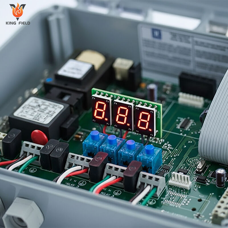
8. PCB Assembly Techniques: SMT, Soldering, and Inspection
The rise of wearable PCB assembly and ultra-thin devices has pushed boundaries not just in design, but also in manufacturing. Whether building flexible PCB, FPC, or rigid-flex PCB designs, assembly techniques must ensure reliability, accuracy, and minimal stress on components during and after the process. Let’s explore the state-of-the-art strategies that enable high-yield production of modern wearable electronics PCB solutions.
SMT Assembly for Flexible PCBs and Wearables
Surface Mount Technology (SMT) is the default choice for FPC assembly in wearables, but the process must adapt to the unique properties of flexible printed circuit boards.
Key Adaptations for Flex and Rigid-Flex PCBs:
-
Use of Rigid Carrier Pallets or Jigs:
- FPCs, being thin and bendable, require support during pick-and-place and reflow. Rigid carriers prevent distortion and warping.
-
Vacuum Fixtures or Temporary Stiffeners:
- Temporarily attached to the flex circuit to create a flat, stable base for SMT, then removed post-assembly.
-
Accurate Fiducial Markers and Tooling Holes:
- Essential for precise registration during automated placement (<0.01 mm tolerance for 0201 components).
SMT Component Placement:
- 0201 & Micro-BGAs: Wearables often use some of the world’s smallest SMD components to save space and weight.
- Pick-and-Place Calibration: High-precision machines are required; vision or laser guidance is mandatory for correct orientation and positioning.
- Speed vs. Flexibility: Placement speed may be slower than with rigid boards due to the need for careful handling and avoidance of board flex during placement.
Soldering Techniques and Reflow Profiles for Flexible PCBs
The combination of thin polyimide layers, rolled copper, and adhesives makes FPC assembly uniquely sensitive to temperature and mechanical stress.
Recommended Reflow Profile for Polyimide Flexible PCBs
|
Step
|
Target Parameter
|
Notes
|
|
Ramp Up
|
1.0–1.5 °C/s
|
Minimizes thermal gradient
|
|
Soak Zone
|
150–180 °C, 60–120 s
|
Even heating, activates flux
|
|
Peak Temp
|
220–230 °C
|
Standard for ENIG, OSP finish
|
|
Time Above Liquidus
|
50–70 s
|
Ensures full solder wetting
|
|
Cool Down
|
≤3.0 °C/s
|
Avoids thermal shock, warping
|
- Low-Temperature Solder (e.g., Sn42Bi58): Used to protect adhesive layers and prevent delamination in sensitive designs or where temperature-sensitive components are present.
- Nitrogen Reflow: Inert nitrogen environment prevents oxidization during soldering, critical for ultra-fine pads and improving joint quality.
Advanced Processes and Tools
Underfill and Reinforcement
- Underfill: Applied beneath large or sensitive components in flex areas to absorb mechanical stresses.
- Edge Reinforcement: Local stiffeners or thickened coverlay give pierce-resistance or support for connector zones.
Conductive Adhesives
- Used for temperature-sensitive or organic substrates where traditional soldering may damage the board.
- Provide lower-profile joints that maintain flexibility.
Inspection and Testing
Defect detection is more challenging on flexible PCBs, so advanced inspection techniques are crucial.
Automated Optical Inspection (AOI)
- High-magnification AOI: Detects solder bridges, tombstoning, misalignment on micro-scale components.
- X-ray Inspection: Essential for BGAs, micro-BGAs, and fine-pitch hidden joints—invaluable for HDI wearable PCB assemblies.
- Flying Probe Testing: Used for open/short detection where ICT fixtures are impractical for high-mix, low-volume runs.
Flex-Cycle and Environmental Testing
- Dynamic Bending Rigs: Subject assembled boards to thousands of flex cycles to ensure joint and trace durability.
- Humidity and Salt Fog Testing: Validates conformal coating for PCBs, ensuring resilience in sweat-rich or humid environments.
Case Study: SMT Assembly for Wearable Fitness Tracker
A major wearable manufacturer adopted the following steps for their ultra-thin fitness tracker:
- Mounted FPCs to custom-milled stainless-steel carriers to maintain planarity.
- Used AOI and X-ray inspection after each SMT stage.
- Employed a peak reflow temperature of 225°C and time above liquidus of 60 sec, optimized to avoid adhesive burn-through.
- Performed 10,000 flex-cycle tests to simulate 2 years of daily bending; zero solder cracking observed in production lots where underfill was applied.
Quick SMT and Soldering Checklist for Flex/Rigid-Flex Wearable PCBs
- Always use a rigid or vacuum carrier.
- Calibrate pick-and-place for flex-specific jog.
- Follow manufacturer’s recommended ramp, soak, and peak temperature profiles.
- Opt for low-temp solder on sensitive stack-ups.
- Validate all joints with AOI and X-ray, especially for micro-BGAs.
- Consider underfill or stiffeners in high-stress connector zones.
- Simulate lifecycle bending/testing before mass production.

9. Protection Against Moisture, Shock, and Corrosion
In the demanding environment of wearable devices, robust protection strategies are just as important as smart design and precise assembly. Sweat, rain, humidity, body oils, and daily movement subject every PCB for wearables to corrosive, flexural, and impact stress. Without proper protection, even the most advanced flexible PCB or rigid-flex assembly can suffer from performance degradation, short circuits, or even catastrophic failure within months. Let’s dive into the industry-proven ways to shield flex PCB assembly for long, reliable lifespans in real-world use.
Why Moisture and Corrosion Protection Matters
Wearable electronics PCB assemblies are regularly exposed to sweat (containing salts, acids, and organic molecules), ambient humidity, and skin contact. Key failure modes include:
- Moisture absorption: Decreases insulation resistance, causes leakage paths and electrical shorts.
- Corrosion: Eats away copper traces and solder joints, especially in the presence of chloride-rich sweat.
- Delamination: Swelling or hydrolysis of adhesive layers, leading to separation and mechanical failure.
- Mechanical stress: Repeated flexing can lead to micro-cracks in exposed traces and solder joints, further accelerated by moisture ingress.
Conformal Coating for PCBs: Types and Selection
Conformal coatings are thin, protective films applied over assembled PCBs. Their main roles are to exclude moisture and corrosive agents, insulate against arcing or shorts, and sometimes provide a barrier against abrasion or physical impact.
Common Coating Types:
|
Coating Type
|
Key Features
|
Typical Applications
|
Notable Drawbacks
|
|
Parylene
|
Pin-hole free, ultra-thin, uniform coverage, biocompatible
|
Medical/implantable wearables
|
More expensive, needs vapor deposition
|
|
Acrylic
|
Cost-effective, easy masking, fast cure
|
Consumer fitness devices
|
Medium chemical resistance
|
|
Silicone
|
Excellent flexibility, thermal/EHV endurance
|
Rugged, outdoor wearables
|
Longer cure, thickness
|
|
Urethane
|
Good solvent resistance, abrasion
|
Harsh industrial wearables
|
Harder to rework/repair
|
Selective Coating and Encapsulation
- Selective application: Only areas exposed to sweat or environmental risks are coated, leaving heat-sensitive or test points uncoated for manufacturability and diagnostics.
- Potting/Encapsulation: In some rugged devices, critical board zones or components are directly potted with silicone or epoxy encapsulants, providing mechanical shock and moisture barriers.
Strategies for Moisture and Corrosion-Resistant Stack-Ups
- Sealed edges: Coverlay films should tightly wrap the circuit, with minimal exposed copper at the edges. When required, edge sealing with resin or conformal coating is used.
- No-exposed vias: All vias in flex regions should be tented or filled to prevent direct sweat ingress.
- Surface finish selection: ENIG and OSP finishes enhance corrosion resistance; avoid HASL in wearable segments due to uneven application and higher susceptibility to undercutting.
Shock, Vibration, and Mechanical Durability Enhancements
- Stiffeners: Applied around connector regions absorbing plug-in force, or where the FPC meets hard plastics.
- Underfill: Injected beneath large components bridges the mechanical compliance gap, reducing risk of solder joint cracking under repeated bending.
- Reinforced coverlay: Increases local puncture and abrasion resistance, especially vital for thin, skin-contacting devices.
Testing Protocols for Robustness
-
Wearable PCBs undergo:
- Flex-cycle testing: Thousands to tens of thousands of flexes.
- Humidity and salt fog testing: Exposure to ~85% RH, >40°C for days to weeks.
- Drop/shock testing: Simulations of falls or sudden knocks.
|
Test Type
|
Minimum Standard
|
Failure Mode Detected
|
|
Flex-cycle
|
10,000 cycles 30 mm bend, 1 Hz
|
Crack, open trace, delam
|
|
Salt fog (IEC 60068-2)
|
48–96 hours exposure
|
Green copper corrosion, shorts
|
|
Drop test
|
1.2 meter, 10 drops
|
Detachment, solder joint fail
|
10. Power Management and RF Optimization
Power efficiency and robust wireless performance are essential pillars of successful wearable PCB assembly. Low battery life or unreliable connectivity are frequent sources of consumer complaints and failed product launches, making power management and RF (radio frequency) optimization central to your design strategy. Let’s explore how the right flexible PCB and rigid-flex PCB layout, stack-up, and component selections ensure energy-efficient, high-performing, and interference-resistant wearable electronics PCB.
Power Management Tips for Wearable Devices
1. Wide Power Traces and Solid Ground Planes
- Trace Resistance Matters: Minimize voltage drops and resistive losses by using the widest allowable power and ground traces—ideally ≥0.2 mm wide wherever possible on an FPC stack-up. Thin copper or narrow traces quickly sap the efficiency of low-voltage lithium battery systems.
- Solid Planes: In multilayer flex and rigid-flex designs, route ground and power as continuous planes. This approach reduces EMC/ESD susceptibility and lowers IR losses, which is crucial in devices that wake frequently and communicate wirelessly.
2. Decoupling and Power Integrity
- Careful Decoupling Placement: Place capacitors as close as possible to power/ground pins and LDOs/Buck regulators.
- Short, Broad Connections: Use the shortest possible traces between capacitors and IC pads to suppress noise and ripple.
3. Low-Dropout and Switching Regulators
- LDOs for Ultra-Quiet Power: Analog/RF sections typically use LDOs for low-noise, if at the expense of some efficiency.
- Switching Regulators for Efficiency: Digital and sensor platforms favor switchers for high efficiency at the cost of more complex layout (higher-frequency switching noise; careful PCB planning and shielding required).
4. Segmented Power Rails
- Switched Power Domains: Use load switches or MOSFETs to cut off power to sections (e.g., sensors, Bluetooth, displays) when idle, preventing trickle current drain in sleep mode.
- Battery Gauges: Placing battery gauges at the main FPC input simplifies system-level SOC measurement and allows for smart-charging protocols.
RF Optimization for Wearable PCB Assembly
Wearables live and die by their ability to communicate reliably. Whether it’s Bluetooth for headphones, Wi-Fi for patient monitors, or NFC for contactless payment, RF design in flexible PCB assemblies must combat a myriad of integration headaches.
1. Controlled Impedance and Trace Design
-
Impedance Matching: Maintain 50 Ω characteristic impedance on RF traces, using microstrip or coplanar waveguide structures as suggested by chip vendors.
- Adjust trace width, spacing to ground, and PCB stack-up according to an impedance calculator.
- Short, Direct RF Runs: Keep antenna feed lines as short and direct as possible to minimize insertion loss and signal distortion.
2. Antenna Clearance and Placement
-
Clearance is Key: Provide at least 5–10 mm clearance around antennas, free of copper, ground, and large components.
- For small FPCs, employ printed antennas on the flex region—these flex with the device and require robust tuning/matching.
- No Metal Above/Below: Avoid battery packs, shields, or displays directly over antennas or RF front ends; these can detune the antenna and dampen radiated power.
3. Shielding, Grounding, and Isolation
-
RF Ground Shields: Create ground pours and via fences around RF/digital separation boundaries.
- Employ via fences (rows of vias at 0.5–1.0 mm pitch) to isolate RF zones.
- Digital/RF Isolation: Place digital clock, data lines, and switching supplies away from sensitive RF sections. Use cutouts or isolation slits in ground planes if needed.
Case Study: Bluetooth Module in Fitness Tracker
A prominent fitness tracker design team used a six-layer FPC stack-up with dedicated top and bottom ground planes. The Bluetooth antenna was kept on the extreme tip of the strap’s flex region, giving it a 15 mm copper-free, component-free clearance. Designers used a controlled impedance calculator to ensure the feed trace was precisely matched to 50 Ω.
11. Design for Manufacturability (DFM) Guidelines
Transitioning a brilliant wearable PCB assembly concept into high-volume reality means designing for more than just functionality—manufacturability is a decisive factor. Neglecting DFM for flexible PCBs or rigid-flex structures can lead to production rejects, yield losses, increased costs, or even delayed launch. For wearables, with their tiny, irregular form factors and exacting reliability requirements, every detail in your DFM approach makes a difference.
Core DFM Guidelines for Flexible and Rigid-Flex PCBs
Keep Bend Radius Large Enough
-
Bend Radius ≥10× Thickness Rule: For any dynamic flex zone (a region that will bend during use), the minimum inside bend radius should be 10 times the total thickness of the flex stack-up.
- Example: A 0.2 mm thick FPC should never be bent tighter than a 2 mm radius during normal operation.
- Tighter bends are possible for static applications but always require pre-production cycle testing for qualification.
Avoid Components & Vias in Flex/Bend Areas
-
No components/vias near edges or bendable segments:
- Place all critical/sensitive parts on rigid zones or far from bend axes.
- Rule of thumb: Keep a buffer of at least 1 mm between the nearest component/via and the start of a dynamic bend.
- Tented or filled vias only: Prevents wicking of flux or later ingress of moisture/corrosion.
Include Fiducials, Tooling Holes, and Registration Features
- Fiducial Markers: Provide clear points for SMT alignment—critical for precision assembly, especially with 0201 parts.
- Tooling holes: Facilitate accurate placement on assembly carriers, essential for high-speed automated flex assembly.
Maintain Copper and Stack-Up Symmetry
- Balanced Copper Distribution: Ensures even mechanical properties and mitigates the risk of board warping or twisting after reflow or flexing.
- Stack Symmetrically: For rigid-flex designs, mirror stack-ups where possible so the board does not “curl” post-manufacturing or coating.
Use Appropriate Stiffeners and Reinforcements
- Rigid areas require reinforcement: Add stiffeners (FR-4 or Polyimide pieces) under SMT connector zones, test pads, or components likely to experience insertion/extraction forces.
Design-for-Assembly Tips for Wearable FPCs
- Pad design: Use non-solder mask defined (NSMD) pads for improved solder joint quality.
- Component spacing: Keep adequate space between SMT devices to allow AOI/X-ray inspection, especially for micro-BGAs.
- Edge clearance: At least 0.5 mm from copper to board outline to avoid shorts, delamination, or poor edge finishes.
Routing Guidelines Table
|
Routing Practice
|
DFM Recommendation
|
Rationale
|
|
Flex region trace width
|
≥0.1 mm (if possible)
|
Increases mechanical life
|
|
Minimum space between traces
|
≥0.1 mm
|
Reduces risk of shorts, delam
|
|
Trace-to-edge distance
|
≥0.5 mm
|
Protects against delamination
|
|
Via pad in flex zone
|
Tented, no via-in-pad unless justified
|
Mitigates moisture, cracks
|
|
Test point in flex zone
|
Avoid; use edge or rigid zone
|
Prevents stress failures
|
Utilizing DFM Analysis Tools
Industry tools from top PCB manufacturers streamline the transition from design to production. Use free/online DFM checkers to flag manufacturability risks before releasing gerbers to your flex supplier.
- JLCPCB DFM Tool: Web-based, supports flex, rigid, and rigid-flex designs.
- ALLPCB/Epec DFM Analyzers: Include flex design stack-up libraries, common IPC rules, and can simulate manufacturing process steps.
- In-house DFM checks: Many EDA tools support rule-based flex and rigid-flex DFM analysis—activate and customize as early as possible in layout.
DFM Review Checklist
- Confirm all intended bends meet minimum radius.
- No components or test pads in bend/flex regions.
- Stack-up balanced and symmetrically layered.
- Fiducials and tooling holes on every panel.
- Stiffeners specified under connectors and high-force locations.
- All DRs (Design Rules) are DFM-checked by supplier before mass fab.
Example: Avoiding Costly Mistakes
A leading wearables startup failed to account for bend radius and via placement in their first-generation fitness patch, resulting in a 32% board reject rate due to cracked traces and open vias in production run #1. After redesigning with proper DFM, adding a 1 mm via-to-bend buffer and increasing minimum bend radius to 8× thickness, yields increased to 98.4% in the next lot and warranty claims disappeared.
12. Common Failures in PCB Assembly and How to Prevent Them
Despite advances in materials, assembly, and design automation, the real-world performance of wearable PCB assembly is often dictated by a handful of recurring—and preventable—failure modes. Understanding the root causes and implementing best-practice prevention strategies is essential to avoid costly recalls, returns, or dissatisfied customers. This section details the most common failure mechanisms encountered in flexible PCB and rigid-flex PCB manufacturing, and outlines proven, actionable solutions.
Solder Cracking and Fatigue
What goes wrong: As flexible printed circuit boards undergo repeated bending—sometimes thousands of flex cycles in daily wearable use—stress accumulates at SMB solder joints, especially on bend axes or in areas with high strain differentials. Eventually, small cracks can form in the solder, leading to resistive connections or catastrophic opens.
Why it happens:
- Placement of components on or near dynamic bend regions.
- Use of brittle solder alloys or failure to use underfill where needed.
- Excessive temperature exposure during assembly/rework (leading to microstructural grain growth or stress risers).
- Poor flex/rigid joint design, concentrating stress at one edge.
How to prevent:
- Always place large or rigid components away from bend axes—ideally, in rigid zones.
- Apply underfill beneath BGA, QFN, or large components in flex areas to disperse and absorb mechanical stress.
- Use flexible solder alloys (e.g., those with higher silver content for ductility).
- Simulate flexing during the prototyping phase (flex-cycle testing to >10,000 cycles).
- Design gentle layer transitions (no abrupt steps between rigid/flex zones).
Delamination and Adhesive Separation
What goes wrong: Layers of the FPC or rigid-flex board separate—either along the copper-polyimide interface, within the adhesive layer, or under coverlay in high-moisture environments. Delamination is often catastrophic, leading to immediate circuit disconnection.
Key causes:
- Trapped moisture during assembly (not pre-baking flex boards).
- Too-high reflow temperatures degrading adhesives.
- Poor copper-to-PI adhesion due to contamination or incorrect stack-up sequence.
- Assembly stress on layers due to improper stiffener attachment.
How to prevent:
- Always pre-bake flexible PCB panels (125°C, 2–4 hours) before SMT assembly to drive off absorbed moisture.
- Use low-temperature solder and tune reflow profiles to avoid adhesive decomposition.
- Specify high-quality polyimide and proven adhesive systems.
- Careful stiffener design/application—applied with compliant films, not hard adhesive beads.
Table: Delamination Prevention Checklist
|
Step
|
Action
|
Impact
|
|
Moisture control
|
Pre-bake boards
|
Prevents vapor bubbling, layer lift
|
|
Adhesive selection
|
Qualified vendor, correct type
|
Ensures thermal cycle stability
|
|
Reflow temp management
|
Low-temp solder/reflow
|
Avoids adhesive/film burn-off
|
|
Cleanliness
|
No flux/grease in layup
|
Maintains bond quality
|
Corrosion and Moisture Ingress
What goes wrong: Unprotected copper traces, vias, or pads corrode—especially in sweat-prone devices—leading to green copper salts, high resistance, open circuits, or dendritic shorts.
Root causes:
- Incomplete or poorly applied conformal coating.
- Wicking at exposed/unfilled vias in flex regions.
- Unsealed edges or delaminated coverlay.
- Poor choice of surface finish on exposed pads (HASL instead of ENIG/OSP).
How to prevent:
- Select robust conformal coating (parylene, acrylic, silicone) for environmental sealing.
- Tented/fill all vias in flex zones; avoid unnecessary through-holes.
- Edge sealing and continuous coverlay wrap of flex PCBs.
- Use ENIG or OSP surface finishes proven for corrosion resistance in wearables.
RF Drift and Wireless Failures
What goes wrong: A device that works in the lab loses range or suffers intermittent Bluetooth/Wi-Fi performance “in the wild.” Often, reworking or coating the device shifts antenna resonance or increases insertion loss.
Common causes:
- Inadequate or non-repeatable antenna clearance.
- Ground pour or shield placed too close to the antenna/trace after redesign or as a patch.
- Incorrect stack-up or uncontrolled impedance on RF lines.
- Coating too thick or with the wrong dielectric constant applied over antennas.
How to prevent:
- Keep 5–10 mm clearance around the antenna at both layout and assembly.
- Careful impedance control: Always use stack-up calculators and test assembled impedance in production.
- In-situ antenna tuning: Final tuning must be done after all coatings and enclosure assembly.
- Establish RF test as a production outgoing QC item, not just a design-phase checklist.
Quick Reference Prevention Table
|
Failure Mode
|
Prevention Action
|
Industry Standard/Tip
|
|
Solder cracking
|
Placement, underfill, flex alloys
|
No comp/via in bend zone
|
|
Delamination
|
Pre-bake, low-temp process, clean
|
Bake at 125°C/2hr, inspect adhesive
|
|
Corrosion
|
Full conformal, ENIG/OSP, no via exp
|
Parylene, tent via, coverlay wrap
|
|
RF drift
|
Clearance, impedance, in-situ tune
|
50 Ω, >5 mm antenna clearance
|
Flex-Cycle and Lifetime Testing is Mandatory
For any design intended for wearable or flex-use, pre-production samples must undergo accelerated flex-cycle, drop, humidity, and salt-fog testing. Results from these tests should drive iterative design improvement—long before mass production.
In summary: Most failures in FPC assembly and rigid-flex PCB builds stem from overlooked fundamentals—placement, moisture management, coating, and electrical design integrity. If you proactively engineer for these points, you’ll deliver best-in-class wearable electronics PCB that thrive in the real world—not just in the lab.
13. Future Trends in Flex and Rigid-Flex PCB Manufacturing
The world of wearable PCB assembly and flexible electronics is evolving at breakneck speed. As consumer and medical devices push for ever-smaller, smarter, and more durable forms, the next wave of innovations in flexible PCB and rigid-flex PCB design and manufacturing are set to transform not just wearables, but the entire electronics industry. Let’s look at the most significant emerging trends poised to shape the future of wearable electronics PCB technology.
1. Advanced Materials: Beyond Polyimide
- Graphene and Nanomaterial Substrates: The introduction of graphene and other 2D materials is expected to open new frontiers for ultra-thin, high-conductivity, and highly flexible circuits. Initial studies show superior flexibility, increased current capacity, and potential for integrated biosensor or stretchable display applications (think electronic skin patches or soft robotics).
- Stretchable Polyimide Blends: New variants of polyimide with built-in stretch and rebound properties will allow PCBs to endure not just bending, but also stretching and twisting—suiting next-gen medical wearables that conform to moving joints, or smart sports apparel.
- Bio-compatible and Biodegradable Substrates: For implants and eco-friendly disposables, research is advancing into materials that degrade safely after use or remain inert in the body long-term.
2. 3D-Printed and Rapid Prototyping Flexible PCBs
- 3D-Printed PCB & Interconnects: The combination of additive manufacturing and functional inks now allows direct printing of entire circuit stacks, antennas, and even rigid-flex hybrids in a single process. This slashes prototype time from weeks to hours and unleashes creativity in the formation of organic or embedded layouts.
- Personalized Medtech Devices: Clinics and research hospitals will soon rapidly print custom patient-worn monitors, matching anatomy or medical needs exactly—dramatically reducing costs and improving patient outcomes.
3. High-Density and Multilayer Integration Growth
- Increased Layer Counts: As smartwatches and medical devices demand more features in the same (or smaller) space, the industry is trending rapidly towards 6-layer, 8-layer, or even 12-layer flexible PCB stack-ups using ultra-thin copper (to ~9 µm) and super-fine dielectrics.
- Ultra-Fine Pitch and Microvia Technology: Microvias as small as 0.05 mm and component pitches under 0.3 mm are set to become routine, enabling stacking of ever more sensors, memory, and power management ICs within millimeter-scale footprints.
- System-in-Package (SiP) & Chip-on-Flex: Direct mounting of bare die (chip-on-flex), multi-chip modules, and integrated passives on flexible substrates will reduce size and boost function in wearables.
4. Integration with Stretchable and Textile Electronics
- Textile Embedding: Wearable electronics are increasingly interwoven with clothing (smart shirts, socks, and patches), where flexible circuits or rigid-flex structures can be encapsulated or sewn directly into fabrics for seamless user experiences.
- Stretchable Circuit Innovation: Metal meshes, serpentine traces, and substrate engineering are making truly stretchable circuits—capable of 20–50% elongation—a reality for fitness and medical devices that must flex, twist, and stretch with the body without losing function.
5. Automated Test, Inspection, and AI-Driven Yield Enhancement
- Smart Factory Integration: Manufacturing lines for flexible PCB assembly are now adopting AI-based inspection (AOI, X-ray, and flying probe testing) to spot micro-defects, predict failures, and optimize yields.
- Cycle Testing as a Standard: Automated flex-cycle and environmental test rigs will soon become standard, ensuring every lot of wearable electronics PCB meets functional lifespan requirements—not as an add-on, but embedded in the process.
6. IoT and Wireless Expansion
- Seamless Connectivity: With 5G, UWB, and emerging IoT protocols, wearable PCBs will integrate more antennas, advanced RF switching, and even self-healing or frequency-tunable traces to optimize performance in dynamic conditions (sweat, movement, environmental changes).
- On-Board Energy Harvesting: Next-gen FPC layouts are already exploring embedded solar, triboelectric, or RF energy-harvesting elements, extending device runtime or even enabling battery-free smart patches.
Industry Perspective and Quotes
“We’re moving beyond simple flex; next-gen PCBs will be soft, stretchable, and almost invisible to the user. The divide between board and product is disappearing.” — R&D Director, Wearable Technology, Top-5 Tech OEM
“Every leap in substrate tech—graphene, stretchable polyimide—doesn’t just shrink the device. It spawns whole new categories of products: smart tattoos, woven sensors, biosensor pills, and beyond.” — Lead Materials Scientist, Medical Device Innovator
Table: Future-Ready Features Coming to Flexible and Rigid-Flex PCB Manufacturing
|
Feature / Trend
|
Impact on Wearables
|
Timeline
|
|
Graphene Substrates
|
Ultra-thin, highly flexible, strong
|
Early adoption now, widespread by 2030
|
|
3D-Printed Flex-PCBs
|
Rapid prototyping, customization
|
First commercial 2025-2027
|
|
Stretchable Electronics
|
Conformality, biomechanical fit
|
2026 and beyond
|
|
Multilayer HDI
|
Higher function in tiny space
|
Already common, rising through 2030
|
|
Textile Integration
|
Invisible/ubiquitous electronics
|
Emerging now, mainstream by 2028
|
|
AI-Powered Yield
|
Lower cost, higher reliability
|
In use at top manufacturers, expanding
|
14. Conclusion: Why Flex and Rigid-Flex PCBs Power the Next Generation
The journey through wearable PCB assembly—from core materials and stack-up strategies to nuanced assembly, protection, and future trends—reveals a single underlying truth: flexible PCB and rigid-flex PCB technologies are the foundation upon which the next decade of wearable and medical innovation will be built.
The Key to Miniaturization and Functionality
Whether it’s a discreet health patch or a feature-rich smartwatch, miniaturization defines modern wearables. Only flexible printed circuit boards and their rigid-flex cousins can fully exploit the available space, winding through curves, layering critical functionality in less than a millimeter of thickness, and delivering featherweight comfort to end-users.
Table: Summary—Why Flex and Rigid-Flex Win for Wearables
|
Advantage
|
Flexible PCB
|
Rigid-Flex PCB
|
|
Maximum bendability
|
✓✓
|
✓
|
|
Ultra-lightweight
|
✓✓
|
✓
|
|
Complex shapes/layouts
|
✓✓
|
✓
|
|
Reduced interconnects
|
✓
|
✓✓
|
|
Multi-axis reliability
|
✓
|
✓✓
|
|
High-speed signals/RF
|
✓
|
✓✓
|
|
Assembly yield & scale
|
✓
|
✓
|
Reliability and Product Longevity
Wearables are subject to thousands of cycles of flexing, perspiration, shock, and daily wear. Only through careful FPC assembly, conformal coating, smart component placement, and validated DFM rules can you avoid the pitfalls that doom lesser designs. The most successful, reliable products in the marketplace all follow these essential practices—yielding true commercial success and delighted users.
Driving Performance and Power Management
From battery life to RF performance, PCB for wearables sets the bar. The intricacies of impedance control, noise suppression, and integrated low-power circuitry made possible by the latest manufacturing techniques ensure that wearables perform strongly while sipping power from tiny batteries.
Enabling Revolutionary Applications
Rigid-flex PCB and advanced flex circuits not only serve today’s needs—they open the door for tomorrow’s breakthroughs:
- Smart medical patches that continuously monitor patient health
- Fitness devices that can disappear into clothing or the body
- AR/VR modules that are unobtrusive, lightweight, and almost weightless
- IoT and AI-enabled wearables with real-time communication, energy harvesting, and embedded intelligence
All About Collaboration
Finally, harnessing the full power of wearable electronics PCB solutions—especially for mass-market or regulatory-sensitive applications—means working with expert partners in PCB manufacturing, assembly, and testing. Utilize their DFM tools, embrace real-world testing prior to product launch, and treat lessons from the field as fuel for continuous improvement.
 Hot News