Introduction
In today’s fast-paced electronics industry, speed is king. Catching and correcting design errors as early as possible plays a crucial role in product success and business profitability. For many engineers and manufacturers, traditional PCB manufacturing timelines simply can’t keep up with the demand for rapid product development and short time-to-market cycles. This is where quick-turn PCB prototypes emerge as a critical asset for companies seeking to innovate and iterate faster, with minimal risk and maximum efficiency.
Understanding Quick Turn PCB Prototypes
In the realm of electronics innovation, quick-turn PCB prototypes have become synonymous with agile engineering and high-speed product development. But what exactly makes a quick-turn PCB prototype different from a conventional PCB? Understanding this distinction—and appreciating the nuances involved—will help you make informed decisions that can dramatically impact your project’s timeline and success.
What Is a Quick-Turn PCB Prototype?
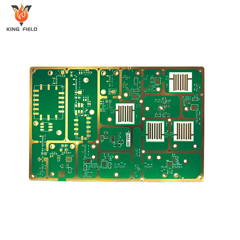
A quick-turn PCB prototype is a printed circuit board manufactured and assembled within an accelerated timeframe—often within 24 hours to 7 days, compared to the traditional industry lead time of several weeks. The goal is to produce small batches of PCB prototype boards quickly for the purposes of testing, electronic design validation, and design iteration. These are commonly used prior to mass production runs, enabling engineers to catch errors and optimize designs for manufacturability at a fraction of the time and cost.
How Does It Work?
- Focus on Speed: Manufacturers allocate dedicated lines or “express” resources, optimizing the PCB prototyping process from design file review through assembly.
- Iterative Process: Because turnaround is so fast, engineers can complete multiple design iterations in days rather than months.
- Application Scope: Especially valuable in IoT prototyping, wearable technology, medical device design, automotive electronics, and other fast-moving sectors.
Why Do Engineers and Manufacturers Choose Quick-Turn PCB Prototypes?
1. Fast Development Cycles: Launching a new hardware product means multiple rounds of prototype builds to perfect the design and the user experience. Quick-turn prototypes massively compress this loop, allowing teams to move from idea to tested prototype rapidly.
2. Rapid PCB Prototyping for Validation: Before committing to expensive mass production tooling and assembly, engineers need to validate that the board works as intended—both electrically and mechanically. Quick-turn PCB manufacturing supports fast, cost-effective validation cycles.
3. Flexible Problem-Solving: Changes to circuit layout, component selection, or stackup can happen at any stage. With standard processes, these changes become costly and time-consuming. Quick-turn PCB fabrication allows for immediate implementation and testing of design updates—including adjustments to SMT, THT, or even specialty rigid-flex PCB layouts.
4. Early Detection of Errors: PCB prototype manufacturers offering rapid turnaround often include robust DFM (Design for Manufacturability) checks and support. These prevent costly errors—such as incorrect pad sizes, unmanufacturable traces, or component misplacement—before they derail later production.
5. Competitive Advantage: The electronics industry is full of fast followers and market disruptors. Being the first to solve a problem or introduce a feature often equals market share. Quick-turn PCB prototypes provide a tangible business advantage.
Key Features of Quick-Turn Flex Circuits Accelerate Product Development
Quick-turn PCB prototypes have revolutionized the way engineers and manufacturers approach product development and validation. Beyond just speed, these agile prototyping solutions come packed with features that can distinctly accelerate your brand’s journey from concept to commercial launch. Understanding the nuanced capabilities of quick-turn PCB manufacturing makes all the difference when selecting the right rapid prototyping service for your next big project.
1. Ultra-Fast Turnaround Times
Speed is the defining hallmark of any quick-turn PCB prototype service. Leading manufacturers—such as Imagineering PCB, PCBnet, and Sierra Circuits—offer turnaround options that can deliver fully fabricated and assembled PCB prototype boards in as little as 24 to 48 hours for standard builds. For more complex boards, timelines might extend to 3–7 days, yet still drastically cut development cycles compared to standard mass-production PCB runs.
Typical Quick-Turn Turnaround Table
|
Board Type
|
Layers
|
Turnaround (Fabrication Only)
|
Turnaround (With Assembly)
|
|
Rigid PCB
|
1–6
|
1 day
|
2 days
|
|
Rigid PCB
|
8–12
|
3 days
|
4 days
|
|
Rigid-Flex PCB
|
1–12
|
5–7 days
|
6–8 days
|
|
Flex PCB
|
1–10
|
3–5 days
|
4–6 days
|
2. High Flexibility for Iteration and Customization
Quick-turn PCB fabrication is purpose-built for adaptation. Need to change a via size, experiment with a new SMT or THT component, or test a revised stack-up with controlled impedance? Unlike mass production—where change orders are disruptive and costly—quick-turn assembly lines are set up for rapid re-spins and small-volume runs. This gives engineers an unprecedented freedom to experiment and refine without risking project schedules.
- Iteration: Integrate feedback on-the-fly from each test cycle.
- Customization: Mix and match technologies—like surface finish (HASL, ENIG), advanced substrates (FR-4, polyimide), or layer counts—based on your design’s needs.
3. End-to-End Visibility and Communication
Top-tier quick-turn PCB prototype manufacturers are known for transparent communication and project tracking. Dedicated account managers, live engineering chat, and real-time order status portals minimize uncertainty. You know exactly when your Gerber files are under review, when material selection and inventory checks are completed, and when your boards are en route.
- Status Tracking: Online dashboards detail every step—from BOM verification through assembly.
- Proactive DFM Feedback: Fast flagging of any manufacturability issues ensures the latest design version is always buildable.
4. Comprehensive Design for Manufacturability (DFM) Support
One reason quick-turn PCB prototyping is so successful is its robust focus on DFM guidelines. With every order, experienced engineering teams perform automated and manual DFM checks to catch common issues:
- Minimum trace width/spacing violations
- Incompatible drill sizes or unsupported via-in-pad requests
- Footprint mismatches between BOM and centroid files
- Panelization review for optimal fab efficiency
5. Optimized for Small Batches and ROI
Quick-turn PCB assembly and fabrication are inherently optimized for small- to mid-volume production, focusing on quantities from a single board up to a few hundred units. This model delivers strong ROI through:
- Reduced waste: Only produce what you need for design validation or field trials.
- Lower upfront costs: No need for mass-production tooling.
- Faster feedback: Send small runs for testing and certification as required.
6. Quality Control, Testing, and Compliance
Even when speed is the priority, quality must never be compromised. Premium rapid PCB prototyping services rigorously adhere to IPC Class II and III standards, AS9100D / ISO9001:2015 certifications, and RoHS compliance. They integrate advanced inspection systems:
- AOI (Automated Optical Inspection)
- Flying Probe or ICT (In-Circuit Testing)
- Functional testing for programmable boards
7. Streamlined Shipping and Logistics
Because speed is at the heart of quick-turn PCB manufacturing, shipping and logistics are often expedited as well. Many vendors offer same-day dispatch, real-time logistics tracking, and global express shipping options to ensure your boards arrive on-site ready for immediate validation or demo, regardless of your location.
Feature Summary Table: Why Engineers Choose Quick-Turn PCB Prototypes
|
Feature
|
Benefit to Engineers & Manufacturers
|
|
Ultra-fast turnaround
|
Immediate prototyping for rapid development cycles
|
|
High flexibility
|
Fast re-spins for iterative refinement
|
|
DFM and engineering support
|
Early error elimination, manufacturability optimization
|
|
Quality assurance (ISO/IPC/RoHS)
|
Peace of mind for high-stakes applications
|
|
Optimized for small batch orders
|
Cost-effective product validation, MVP, and field tests
|
|
Transparent communication
|
Real-time updates, proactive troubleshooting
|
The Quick Turn PCBs Prototyping Process Explained
The quick-turn PCB prototyping process transforms your design from idea to a working, testable circuit board—often in less than a week. This process is intentionally streamlined and tightly managed, yet each step is as critical for rapid prototyping as it is for high-volume production. Whether you are developing IoT sensors, wearable devices, or high-reliability aerospace systems, a clear understanding of these steps gives you the power to control costs, quality, and turnaround time.
Below is an in-depth look at the six essential stages in modern quick-turn PCB manufacturing, from digital files to final delivery.
1. Design Files and Specifications
The journey begins with design documentation: the digital instructions manufacturers need to accurately fabricate and assemble your boards.
Required Design Files:
- Gerber Files: The universal "blueprints" detailing all copper layers, solder mask, silkscreen, and board outline.
- Bill of Materials (BOM): Detailed component list, including designators, part numbers (MPN), descriptions, package outlines, and manufacturer preferences.
- Centroid (Pick-and-Place) Files: Precise X/Y data and rotation for SMT and THT component placement.
- Schematic and Assembly Drawings: Visual guides to reinforce the intent and highlight critical features.
- Stack-up and Drill Files: Clear details on layer count, material, controlled impedance requirements, and all hole types.
2. DFM (Design for Manufacturability) Check
As soon as your files are received, the PCB prototype manufacturer initiates a comprehensive DFM review, which may be both automated (software checks) and manual (human expert review).
Key DFM Elements Checked:
- Minimum trace width and spacing for chosen process
- Drill hole diameters & aspect ratios
- Pad/footprint alignment versus BOM
- Panelization setup for fabrication efficiency
- Gerber-BOM-centroid file consistency
- Prohibited or unsupported features (e.g., via-in-pad for fine-pitch BGAs unless explicitly required)
- Stack-up compatibility with available substrate materials
Typical DFM turnaround in quickturn environments:
- Automated review: Minutes to a few hours
- Manual review: 1–8 hours (depends on complexity, can be parallelized for urgent 24-hour cycles)
3. Material Selection and Inventory Check
After your design is verified for manufacturability, the manufacturer reviews the BOM for component sourcing and scans material inventories.
What happens in this step?
- Substrate Material & Stack-up Selection: Standard FR-4 is used for most rapid PCB prototyping, but options like polyimide (for rigid-flex PCBs) or high-frequency laminates (for RF, 5G, automotive) may be available in-stock for premium services.
- Component Availability Check: Involves cross-checking BOMs with internal stock and major distributors. Quickturn-focused vendors maintain a watchlist of common passives (resistors, capacitors), microcontrollers, and connectors.
- Pin-Compatible Alternatives: If a component has long lead times, the assembler may suggest pin-compatible, functionally equivalent parts (with your approval), keeping the prototype on schedule.
Table: Common Quick-Turn Substrate Materials
|
Material Type
|
Applications
|
Typical Availability in Quickturn
|
|
FR-4
|
General electronics
|
Always in-stock
|
|
Polyimide
|
Flex/rigid-flex, wearables, medical
|
1–3 days lead (standard stacks)
|
|
Rogers/PTFE
|
RF, high-freq, 5G, IoT, aerospace
|
2–4 days lead (popular specs)
|
4. Prototype Manufacturing (Fabrication & Assembly)
Once files and materials are cleared, high-speed fabrication and assembly begin.
Fabrication Functions:
- Multilayer board lamination with registered layers and drill hits
- Automated optical inspection of etching, mask, and silkscreen
- Surface finish application (ENIG, HASL, gold, OSP, etc.)
- Laser routing (for complex contours, rigid-flex PCBs)
Assembly Functions:
- SMT Placement: Automated pick-and-place for high-density component population
- THT Insertion & Soldering: For connectors, large passives, and mechanical parts
- Reflow & Wave Soldering: Fast turnaround, high reliability
- X-ray Inspection: Used for BGAs and dense assemblies
5. Quality Control and Testing
Even at lightning speed, quality control remains paramount in quick-turn PCB manufacturing. No prototype is shipped without thorough inspection:
6. Shipping and Delivery
The last mile matters as much as the first. After passing inspection, boards are packaged per ESD standards and dispatched for express shipping.
Common Challenges During Quick Turn Flex Circuits PCB Prototyping and How to Overcome Them
Even with the best tools, planning, and manufacturing partners, quick-turn PCB prototype projects can hit unexpected snags. Rapid timelines compress every step, making even ordinary challenges feel urgent. Fortunately, most manufacturers specializing in quick-turn PCB manufacturing have robust systems in place to help you anticipate, mitigate, and overcome the most common hurdles.
1. Design Compatibility Issues
Nature of the Challenge
When design files don’t clearly convey the designer’s intent—or contain errors such as trace violations or unsupported via types—manufacturers must pause for clarification. In quick-turn projects, these delays can be costly.
Typical Scenarios
- Mismatched Gerber, BOM, and centroid files (e.g., footprint/pad differences, missing components)
- Ambiguous instructions in fabrication or assembly notes
- Incompatible specifications, such as requesting an unsupported solder mask or stack-up in a 24-hour cycle
How to Overcome
- Early Communication: Share your design goals and high-priority areas with your chosen PCB prototype manufacturer.
- DFM Collaboration: Respond immediately to DFM feedback, and treat your vendor’s engineering team as an extension of your own.
- Documentation Best Practices: Use revision-controlled files, standardized naming, and include a clear PCB documentation checklist with every submission.
2. Component Availability
Nature of the Challenge
The global electronics industry still faces ongoing challenges with component shortages, particularly for specialized ICs, MCUs, and certain capacitors/inductors. In quick-turn environments, waiting on a critical part—even for a day—defeats the purpose.
Typical Scenarios
- Out-of-stock resistors, capacitors, or ICs that don’t have drop-in equivalents
- BOMs with obsolete or hard-to-source parts
- Unique connectors or specialized power supplies
How to Overcome
- Design with Readily Available Components: Early in your PCB design optimization phase, use parametric search tools (Digi-Key, Mouser, Octopart) to double-check real-world stock.
- Collaborate on Substitutions: Allow your assembler to suggest and verify pin-compatible, functionally equal alternatives. List approved alternates in your BOM upfront.
- Supplier Partnerships: Work with rapid PCB prototyping services known to maintain robust component inventories—or those with distributor partnerships for same-day sourcing.
3. Timely Shipping and Delivery
Nature of the Challenge
All the speed in manufacturing means nothing if your boards are stuck in transit. Delays commonly result from customs clearance, weather-disrupted logistics, or bottlenecks at either end of the shipping process.
Typical Scenarios
- Customs hold-ups when importing/exporting prototype PCB boards
- Incomplete, inaccurate shipping documentation (vendor or engineer side)
- Poor tracking or lack of advance notification
How to Overcome
- Vet Your Manufacturer’s Logistics: Choose a PCB prototype manufacturer with a proven on-time record, solid logistics partners, and transparent shipping practices.
- Onshore/Local Manufacturing for Urgent Cycles: When speed is truly critical, local quick-turn PCB assembly (within the USA, for U.S. customers; Europe for EU customers) can cut end-to-end time by days.
- Preparation: Double-check your shipping address, provide any required import paperwork early, and keep communication lines open with both vendor and courier.
A Quick Reference Table: Common Quick-Turn Pitfalls & Solutions
|
Challenge
|
Typical Issue
|
Solution
|
|
Design Compatibility
|
File conflicts, DFM violation, unclear intent
|
Early comms, DFM best practices, documentation
|
|
Component Availability
|
Parts not in stock, supplier delays
|
Use common parts, approve substitutions, multiple sources
|
|
Shipping & Delivery
|
Customs, paperwork, shipment errors
|
Onshore fab, validated address, proactive tracking
|
Advantages of Quick-Turn PCB Prototype Boards
Adopting quick-turn PCB prototypes in your product development process delivers far-reaching benefits. These advantages go beyond simply getting test boards faster; they impact every stage of the innovation cycle—lowering cost, reducing risk, and accelerating your path to market leadership. Let’s dissect the top five reasons why engineers and manufacturers are increasingly turning to rapid PCB prototyping and quick-turn PCB manufacturing.
1. Accelerated Product Development
Quick-turn PCB fabrication slashes the length of every prototype iteration. What previously took weeks can now be accomplished in days, enabling engineering teams to:
- Validate new concepts rapidly: Early testing is crucial before investing in tooling or large-scale manufacturing.
- Experiment and innovate: Try multiple layouts, IC footprints, or stack-ups in succession, quickly refining the design.
- Compress the R&D calendar: Accelerated cycles mean more time for hardware-software integration, end-user testing, or parallel feature development.
2. Reduced Time-to-Market
Bringing new technology to market while the opportunity is “hot” is a major competitive advantage. Quick-turn PCB assembly allows companies to:
- Deliver working prototypes for demos, tradeshows, or prospective clients faster
- Secure additional funding or purchase orders based on proof-of-concept hardware
- React to customer feedback or competitor moves with near real-time product updates
Real-World Example
A North American IoT hardware startup used three overnight quick-turn PCB prototype cycles in a single month to adapt to late-breaking customer requests. This responsiveness directly led to winning a six-figure pilot contract—beating two competitors still waiting for overseas prototypes to ship.
3. Faster Iterations and Rapid Testing
Iterative development isn’t just for software. In electronics, it’s about physical validation:
- Test design revisions for signal integrity, EMI/EMC compliance, or power budgets.
- Swap key ICs or layout elements based on preliminary test data.
- Debug edge-case performance issues early with real hardware.
This loop: Design → Prototype → Test → Refine → Re-prototype is at the core of agile electronic engineering. Quick-turn PCB manufacturing enables numerous cycles with minimal downtime, so every iteration delivers measurable progress.
Table: Iteration Speed Comparison
|
Approach
|
Typical Iteration Cycle
|
# Iterations/Month
|
|
Standard PCB Prototyping
|
2–3 weeks
|
1–2
|
|
Quick-Turn PCB Prototyping
|
2–7 days
|
4–10+
|
4. More Efficient Identification of Design Flaws
Catching errors early saves time, budget, and reputation:
- Identify and fix layout mistakes, incorrect footprints, or polarity mismatches before scale-up.
- Verify manufacturability and component fit using actual boards, not just 3D models.
- Run root-cause analysis for observed failures under realistic electrical or environmental test conditions.
5. Mitigated Large-Scale Production Risk
The most expensive errors are those discovered after ramping up production. Rapid PCB prototyping dramatically reduces risk by:
- Proving out DFM and DFA (Design for Assembly) assumptions before committing to expensive custom fixtures or jigs.
- Validating alternate BOMs and substitute suppliers for resiliency and supply chain security.
- Standardizing stack-ups and assembly notes, so scaling to 1,000 or 100,000 units is smoother.
Summary Table: Advantages of Quick-Turn PCB Prototype Boards
|
Advantage
|
Impact Area
|
Real-World Value
|
|
Accelerated Product Development
|
R&D, go-to-market
|
Faster launches, keeps pace with changing trends
|
|
Reduced Time-to-Market
|
Sales, funding
|
Respond instantly to investors, partners, customers
|
|
Faster Iteration and Testing
|
Engineering
|
Quick bug fixes, design enhancements for reliability
|
|
Efficient Flaw Identification
|
QA, compliance
|
Lower risk of mass-production defects
|
|
Mitigated Production Risk
|
Operations, logistics
|
Smoother scale up, proven DFM/DFA processes
|
Designing PCBs for Quick-Turn Prototyping — Best Practices
Optimizing your PCB design for quick-turn prototyping is more than just submitting files sooner; it’s a strategic process that can drastically improve your prototype’s manufacturability, quality, and turnaround time. In fast-paced product development, even the best quick-turn PCB manufacturing partner can only go as fast as your design allows. Engineering with DFM (Design for Manufacturability) and DFT (Design for Test) in mind is critical to leveraging the full power of rapid PCB prototyping.
1. Keep Your Designs Simple and Focused
Minimize complexity where possible, especially in the initial prototype stage. The more straightforward your design, the fewer opportunities there are for errors and bottlenecks.
- Limit Board Layers: Start with essential layers only—4 to 6 layers is optimal for quick-turn services.
- Avoid Non-Standard Features: Exotic geometries, non-standard cutouts, or unnecessary notches often slow down fabrication.
- Use Standard Stack-Ups: Align your layer stack with common, fast-turn configurations.
Quick-Turn Prototype Layer Stack Example
|
Stack Type
|
Typical Use Cases
|
Quick-Turn Friendly?
|
|
2–4 layers, FR-4
|
General prototypes, IoT
|
✅ Yes
|
|
6 layers, FR-4
|
Signal integrity, IoT, RF
|
✅ Yes
|
|
8+ layers, HDI
|
Dense routing, BGA, RF
|
⚠️ Possible delays
|
|
Flex/Rigid-Flex
|
Wearables, med devices
|
Choose std. stacks
|
2. Use Readily Available, Standard Components
Component sourcing is often the slowest link in rapid PCB prototyping.
- Choose Parts in Stock: Check distributors (Digi-Key, Mouser, Arrow) for real-time inventory. Avoid custom or obsolete components.
- Allow for Drop-In Equivalents: Where possible, specify pin-compatible alternatives in your BOM.
- Use Popular Footprints: SOIC, QFP, 0603/0402 passives are easiest for quick-turn SMT lines.
3. Follow DFM (Design for Manufacturability) Guidelines
Proper DFM practices prevent errors and ensure your design passes the manufacturer’s rapid DFM check the first time.
- Maintain Minimum Trace/Space: Adhere to your manufacturer’s design rules—typical minimums for FR-4 are 4/4 mil trace/space.
- Via Design: Avoid via-in-pad or exotic microvias unless expressly supported for fast-turn (may add time/cost).
- Panelization for Prototypes: If you need multiple test units, design for standard panel size and breakaway tabs.
- Clear Silk/Masks: Silkscreen and soldermask should be clear, legible, and match the component placement.
Top DFM Pitfalls to Avoid
|
Pitfall
|
Impact
|
|
Trace width violations
|
Delays, re-spins
|
|
Unsupported via/pad types
|
Increased cost or scrap
|
|
Layer stackup ambiguity
|
Wrong impedance or instability
|
|
Inconsistent file revisions
|
Build wrong version, wasted runs
|
|
Poor documentation
|
Questions, potential build pauses
|
4. Ensure Proper and Complete Documentation
Thorough, clear documentation prevents confusion and delays. For quick-turn PCB manufacturing, include:
- Gerber Files: All copper, mask, silk, and contour layers.
- BOM (Bill of Materials): Complete with MPNs, values, tolerances, package info, and alternates.
- Centroid (Pick-and-Place) Files: X/Y, rotation, refdes for each placed component.
- Assembly Drawings & Notes: Placement orientation, any manual operations required, no-stuff indicators.
- Test & Inspection Criteria: State if flying probe, functional test, or AOI is required.
- Contact Info: Engineering and procurement emails/phones for quick question resolution.
5. Collaborate Early and Often with Your Manufacturer
Early engagement with your PCB prototype manufacturer drastically improves success rates and protects against surprises.
- Request DFM/Stackup Pre-Checks: Submit a preliminary design draft and BOM before you finalize.
- Ask About Material Availability: Confirm substrate, soldermask, and finish options that are truly stocked for quick-turn.
- Real-Time Engineering Support: Use chat or phone hotlines for last-minute technical clarifications or DFM tweaks.
- Accept Feedback Proactively: If your vendor suggests changes, weigh them seriously---their experience can save you time and trouble.
6. Plan for Rapid Test and Debug
Fast prototyping cycles deserve equally fast debugging.
- Include Test Points: Make access to key nets and power rails simple.
- Design for Flying Probe/ICT: Confirm testability for continuity or boundary scan.
- Label Everything: Clearly label power, ground, and key signal nets for oscilloscope or probe access.
Documentation Checklist for Quick-Turn Prototyping (Printable)
|
Document/File Type
|
Essential for Quick-Turn?
|
|
Gerber files (all layers)
|
✅ Yes
|
|
BOM w/ alternatives
|
✅ Yes
|
|
Centroid (pick/place)
|
✅ Yes
|
|
Assembly drawings/notes
|
✅ Yes
|
|
Stack-up & drill chart
|
✅ Yes
|
|
Test/inspection criteria
|
✅ Yes
|
|
Contact information
|
✅ Yes
|
|
Revision history
|
✅ Yes
|
Quick-Turn PCB Manufacturing Process — Example
To fully appreciate how quick-turn PCB prototypes go from concept to reality, it’s valuable to map the journey of an actual board through a rapid PCB prototyping service. This example case offers not just an overview of steps, but hard insights into timelines, decisions, and quality checks that set quick-turn PCB manufacturing apart from standard cycles.
Step-by-Step Quick-Turn PCB Manufacturing Example
1. Submission & Review (Hours 0–2)
The design team uploads their files—Gerber, BOM (Bill of Materials), centroid, stack-up drawing, and assembly notes—to the manufacturer’s quick-turn portal.
- Automated DFM review runs within minutes, checking trace/space, via dimensions, footprints, and design rule compliance.
- Immediate human engineering review highlights small BOM inconsistencies (e.g. a substitute resistor required for one value) and feeds back to the customer.
- Customer approves minor corrections within 1 hour.
2. Material and Component Sourcing (Hours 2–8)
With documentation and DFM cleared, the vendor checks component availability:
- FR-4 core and standard surface finish (ENIG) are confirmed in local inventory.
- All critical ICs, RF module, and most passives are in stock. Only one inductor requires a last-minute change. The assembler suggests a cross with identical form/fit/function.
- Customer signs off, and the BOM is finalized.
3. Fabrication Queue & Pre-Assembly (Hours 8–24)
- Manufacturer queues the job on a dedicated quick-turn fabrication line.
- Core and prepreg materials are pressed and etched into a 4-layer stack.
- Drilling, electroless plating, and imaging proceed in tight sequence.
- Soldermask, silkscreen, and ENIG finishes applied.
- Boards are routed out of the panel, deburred, and moved to assembly.
4. PCB Assembly (Hours 24–48)
- SMT placement populates microcontrollers, RF module, passives, and LEDs.
- THT insertion (connectors, headers) follows using selective soldering.
- AOI (Automated Optical Inspection) passes first time; two boards are flagged for manual check due to silkscreen misalignment (cosmetic, not functional).
- Optional X-ray for the RF module and BGA microcontroller.
- Flying probe test verifies power and major signal rails.
5. Quality Control & Packaging (Hours 48–60)
- Final electrical test and a concise “pass/fail” summary sheet are printed for each unit.
- ESD-safe packaging, labeled as “quick-turn prototype, handle with care.”
- Shipment tracking number and test report emailed to the client.
6. Shipping & Delivery (Hours 60–72)
- Boards dispatched via overnight courier.
- Real-time tracking available through the manufacturer’s portal.
- Engineers receive the boards at their lab, exactly 3 days after submission—ready for firmware loading and field testing.
Quick-Turn Timeline Table
|
Process Stage
|
Duration
|
Notes
|
|
File Review & DFM
|
2 hours
|
Includes customer feedback loop
|
|
Material & Component Check
|
6 hours
|
Alternate sourcing, live inventory check
|
|
Fabrication
|
16 hours
|
High-speed quick-turn line
|
|
PCB Assembly (SMT + THT)
|
16 hours
|
Two shifts for parallel assembly
|
|
Quality Control
|
8 hours
|
AOI, flying probe, manual rework
|
|
Shipping
|
4 hours (prep)
|
Overnight next-day courier
|
|
Total Time
|
72 hours
|
Door to door (lab to lab)
|
Choosing the Right Quick-Turn Fabrication Partner
Selecting the right quick-turn PCB manufacturer is a pivotal step in ensuring the speed, reliability, and quality of your prototypes. Not all PCB fabrication shops are equally equipped for rapid cycles, and the wrong choice can cause costly delays or subpar products—undermining all the advantages of rapid PCB prototyping. Use this section as your blueprint for finding, vetting, and partnering with a fabrication specialist who lives and breathes quick-turn excellence.
1. Location and Manufacturing Capacity
- Onshore Facilities: For the tightest turnarounds, prioritize local or onshore manufacturing. USA-based quick-turn PCB fabrication avoids international shipping, customs delays, and time-zone lags—often shaving days off your project.
- Scalable Capacity: Ensure your partner can handle volumes from a handful of units to hundreds, with consistent quality at every run size.
2. Certifications and Quality Standards
A true rapid prototyping leader will display visible compliance and ongoing certification:
- IPC Class II & III: Minimum standard for most commercial and mission-critical applications.
- ISO9001:2015 / AS9100D: Relates to quality management and aerospace readiness.
- RoHS, ITAR, and UL registration: Demonstrates commitment to regulatory and international export standards.
3. Technical Capabilities and Service Range
Evaluate the mix of in-house expertise, equipment, and service specialties:
- Design for Manufacturability (DFM) & Engineering Support: Must include rapid turn reviews of Gerber/BOM files, detailed feedback, and suggestions for yield improvements.
- Material and Technology Diversity: Ability to support standard FR-4, rigid-flex, polyimide, high-frequency laminates, SMT, THT, and HDI PCB assembly—even on fast cycles.
- Full Assembly Service: Look for end-to-end offerings: sourcing, fabrication, assembly, test, and logistics.
Best-in-Class Tools
- Real-time quoting engines (such as “Turnkey Pro” from Sierra Circuits)
- Automated status tracking and milestone notifications
- Online DFM analyzers and chat-based engineering support
4. Proven On-Time Performance
Speed is only valuable if it’s predictable. The best quick-turn PCB manufacturers stand behind on-time delivery guarantees—with statistics to prove it.
- Ask: What percentage of orders ship on time? Is there a refund or service guarantee for delays?
- Check: Online reviews, testimonials, case studies, and SF delivery performance.
5. Transparency in Communication
Accountability and responsiveness are indispensable for rapid cycles:
- Direct Access: Can you reach support, engineering, or production, not just sales?
- Alerting: Immediate notice of file issues, component shortages, or potential delays.
- Project Dashboard: Status tracking available 24/7 through the quoting/manufacturing portal.
6. Real-World Case Study: Bluetooth IoT PCB
Challenge: A Bay Area IoT company needed a 4-layer, compact Bluetooth mesh gateway to meet VC demo deadlines. After vetting three “quick-turn” suppliers, they chose one with:
- In-house, domestic fabrication and assembly
- 24/7 engineering hotline
- Proven 99% on-time rate (granted by IPC audit)
- End-to-end service from DFM through test and shipping
7. Checklist: How to Vet Your Quick-Turn Partner
|
Evaluation Area
|
Questions to Ask
|
Red Flags
|
|
Certifications
|
Updated IPC, ISO, UL, RoHS?
|
Vague or missing documents
|
|
On-Time Delivery
|
What’s your late shipment rate?
|
No clear answer, <95% on-time
|
|
DFM/QA Support
|
Do you offer rapid feedback and documentation?
|
“We just follow your files”
|
|
Capacity/Scope
|
Can you handle assembly, test, and all layer types?
|
Specialize only in standard PCBs
|
|
Customer References
|
Can I see recent testimonials or case studies?
|
None provided
|
Partnering with Imagineering for Your Quick-Turn PCB Needs
When speed, precision, and reliability are non-negotiable, partnering with a proven industry leader can make all the difference. Imagineering PCB is one of the premier names in the world of quick-turn PCB manufacturing, offering a compelling mix of cutting-edge technology, quality assurance, rapid responsiveness, and customer-first service. Here’s how working with Imagineering unlocks real advantages for engineers and manufacturers aiming for the shortest time-to-market with zero compromises on quality.
Why Choose Imagineering for Quick-Turn PCB Prototyping?
1. Unmatched Speed: Prototypes in as Little as 24 Hours
Imagineering specializes in ultra-fast turnaround times:
- Prototype PCBs shipped in 24 hours for standard rigid boards
- Full-scale production and assembly in 5–7 business days for both simple and complex builds
- Express scheduling and dedicated lines for urgent, high-priority projects
2. Comprehensive Design for Manufacturability (DFM) Support
- Automated and manual DFM checks with every order
- Pre-build collaboration ensures your files are vetted for manufacturing feasibility—no unexpected stalls or re-spins
- Seasoned engineers available to clarify stack-up, layer arrangement, and process-specific queries at short notice
3. Quality and Flexibility for Every Project
- Certified to AS9100D / ISO9001:2015 for quality management and traceability
- Fully ITAR registered, RoHS compliant, and capable of meeting IPC Class II & III inspection criteria
- Handles everything from 1–100,000 units—from MVP prototypes to short-run and full-scale production
4. Advanced Assembly and Inspection Capabilities
- Supports both Surface Mount Technology (SMT) and Through-Hole Technology (THT)
- Can manage rigid, rigid-flex, HDI, and specialty materials (polyimide, FR-4, high-frequency)
- Optional functional, flying probe, and ICT testing for full validation
- Complete Class II & III inspection for mission-critical, aerospace, or medical designs
5. True 100% On-Time Guarantee
Imagineering is one of the few quick-turn PCB manufacturers to publicly stand behind their timelines with a 100% on-time delivery guarantee. If they commit to a deadline, you can depend on it or receive compensation.
Seamless Communication and Customer Tools
- Instant quote engines and online order tracking: Simplifies every project from the first click through delivery
- Dedicated account managers: One point of contact for every question or change request
- Engineering chat and quick-turn hotlines: Get DFM answers or shipment updates in real time
Real-World Success Story: Rapid Iteration for a Medical Device Launch
A global medical electronics provider was facing an accelerated deadline for a wearable telemedicine device:
- Three quick-turn PCB prototype iterations in ten days, each with new stack-up specs and modified analog front ends.
- Imagineering’s engineering review team highlighted a silkscreen-to-pad clearance issue and proposed a fix within two hours.
- Manufacturing, SMT assembly, AOI, and functional test ran over two shifts, so prototypes were hand-delivered to meet a regulatory test event.
- Ultimate result: Device passed clinical validation on time, opening the door for $10M of new business.
Key Services at a Glance
|
Service/Capability
|
Imagineering’s Edge
|
|
Turnaround
|
Prototypes in 24 hrs, production in 5–7 days
|
|
DFM/Engineering
|
Pre-review & troubleshooting, Class III inspection
|
|
Assembly
|
SMT, THT, rigid, flex, rigid-flex, HDI
|
|
Quality System
|
ISO9001:2015, AS9100D, RoHS, ITAR
|
|
Unit Scales
|
1 to 100,000+ with equal quality
|
|
Communication
|
24/7 chat, account managers, live updates
|
|
On-Time Guarantee
|
100% or you’re compensated
|
How to Get Started with Imagineering
Ready to accelerate your next innovation cycle?
- Request a rapid quote: Gather your Gerber files, BOM, and documentation
- Upload to Imagineering’s instant quote portal: Get DFM feedback and discuss options
- Finalize your order: Confirm materials, stack-up, and delivery requirements
- Track your project: Use the web portal or contact your dedicated account manager any time
Frequently Asked Questions (FAQs) About Quick-Turn PCB Prototyping
1. How fast can I get a quick-turn PCB prototype?
Quick-turn PCB fabrication can deliver simple prototypes in as little as 24 hours from final file approval, with most projects completed and shipped within 2–5 business days. Complex multilayer, rigid-flex, or high-density assemblies may require 5–7 days.
Key Factors Affecting Turnaround:
- Number of layers and board complexity
- Assembly (SMT/THT) vs. bare board only
- Component availability and substitutions
- DFM file readiness and response time for clarifications
|
Service Level
|
Typical Turnaround Time
|
|
2–4 layer rigid, bare board
|
24–48 hours
|
|
4–6 layer, full SMT assembly
|
2–3 days
|
|
Rigid-flex, HDI, fine pitch
|
5–7 days
|
2. Can quick-turn prototypes guarantee high-quality PCBs?
Yes—but only if you choose an experienced, certified quick-turn PCB prototype manufacturer. The top rapid PCB prototyping services enforce:
- Full DFM (Design for Manufacturability) review
- Automated Optical Inspection (AOI) and flying probe test
- Assembly to IPC Class II/III standards
- Compliance with AS9100D/ISO9001:2015, RoHS, ITAR, and other certifications
3. What are the limitations of quick-turn PCB prototyping?
- Cost: Quick-turn fabrication and assembly can be more expensive per unit due to dedicated lines and expedited operations.
- Component Constraints: Hard-to-source or custom components may still require substitutions or additional lead time.
- Complexity: Exotic PCBs (many laminations, advanced RF, or ultra-thick boards) may fall outside the fastest turnaround capabilities.
- Documentation: Missing, unclear, or inconsistent files can stall even the fastest prototyping service—ensure your documentation is clean and complete.
4. What are the benefits of quick-turn PCB prototyping?
- Rapid product iteration: Move from design to hardware tests in days, not weeks.
- Faster time-to-market: Outpace competitors with immediate demos, customer pilots, or compliance cycles.
- Lower production risk: Identify and resolve design or assembly flaws before mass production, saving thousands in potential scrap and rework.
- Dynamic response to market change: Pivot quickly as customer or end-user needs evolve.
5. How do I ensure a smooth quick-turn experience?
- Prepare clean, revision-controlled Gerber, BOM, centroid, and assembly files.
- Use standard, in-stock components or provide approved alternates.
- Respond rapidly to DFM and BOM queries from your manufacturer.
- Choose a certified, proven quick-turn PCBA partner with robust references.
Conclusion: Fast-Tracking Innovation with Quick-Turn PCB Prototypes
The demands of today’s electronics industry leave no room for slow, iterative design cycles or delayed product releases. Quick-turn PCB prototypes offer a strategic advantage that goes far beyond speed—they underpin a culture of innovation, risk mitigation, and agile development that drives successful products to market faster, safer, and smarter.
The Power of Quick-Turn PCB Prototyping
By embracing rapid PCB prototyping, companies position themselves to:
- Launch ahead of competitors
- Satisfy demanding customer requirements
- Respond proactively to market shifts
- Dramatically reduce costly late-stage failures
 Hot News