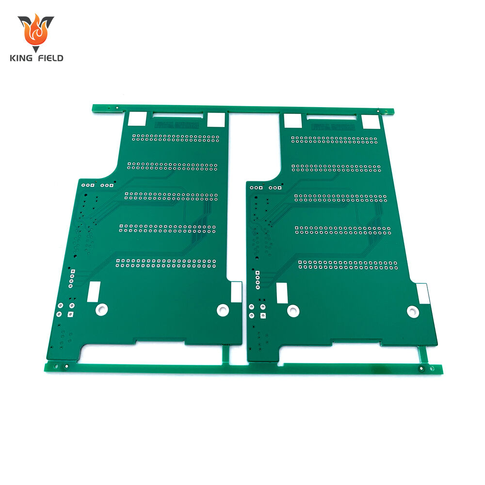
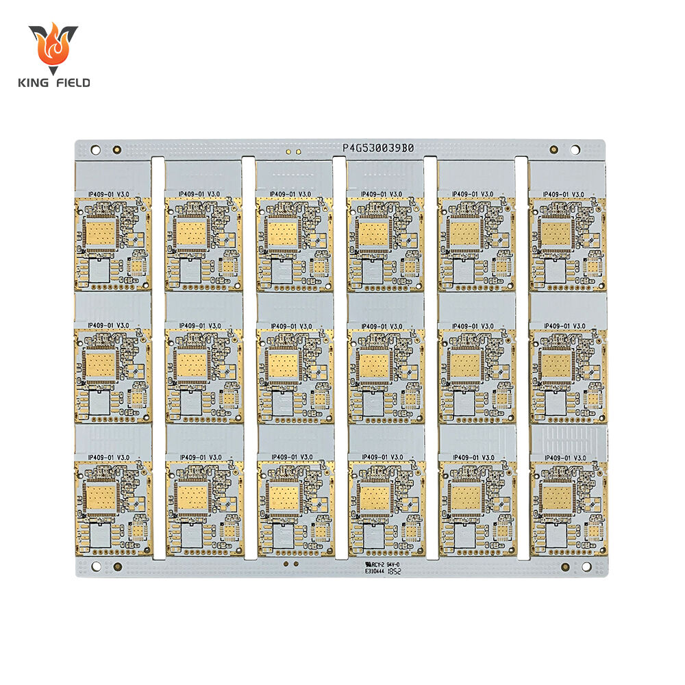
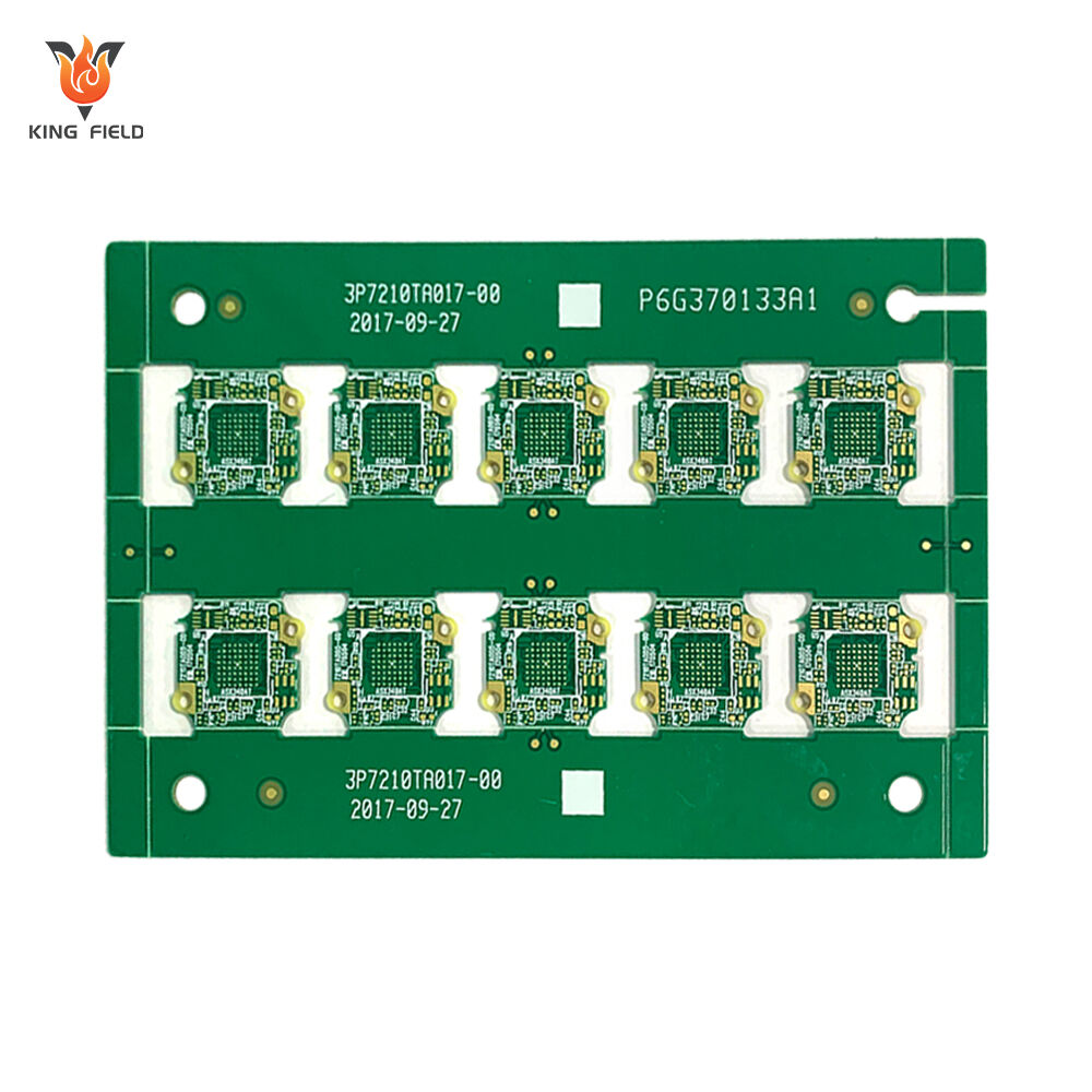
Rigid PCBs
Reliable Rigid PCBs for medical/industrial/automotive/consumer electronics. Stable structure, high durability & precise circuitry—paired with 24h prototyping, fast delivery, DFM support & AOI testing.
✅ Stable, durable design for long-term use
✅ DFM optimization & quality validation
✅ Multi-industry application compatibility
Description
What is a rigid PCB?
Rigid PCB is a printed circuit board made with rigid insulating substrates such as FR-4 epoxy resin glass cloth substrate, phenolic paper substrate or ceramic substrate as the core. It has a fixed shape, high hardness and cannot be bent or folded. It is currently the most widely used type of PCB. Its physical properties are stable, and it has no flexibility at room temperature. It can provide a solid support for components. The mainstream substrate is FR-4, which has a mature process and controllable cost. In high-end scenarios, ceramic or polyimide modified rigid substrates are used to meet the requirements of high thermal conductivity and high frequency. The structure covers single-sided boards, double-sided boards and multi-layer boards, and interlayer interconnection can be achieved through metallized vias. It is compatible with complex circuit designs, has a standardized production process and supports conventional assembly techniques with a high yield rate.
The types of rigid circuit board can be classified based on dimensions such as the number of structural layers, substrate material, and application characteristics. The core classifications are as follows:
Classified by the number of structural floors
· Single panel
It has only one side with conductive copper foil circuits and the other side as the base material. It has a simple structure and the lowest cost, and is suitable for low-power devices with simple circuits (such as remote controls, toy circuit boards, power adapters).
· Double-Sided PCB
Both sides have copper foil circuits, and interlayer interconnection is achieved through metallized vias. The circuit complexity is higher than that of single-sided boards, but the cost is moderate. It is widely used in consumer electronics (mobile phone charging pads), industrial control sensors and other scenarios.
· Multi-layer board
It contains 3 or more conductive layers (commonly 4, 6, 8 layers, and up to 40 layers in high-end models), with the layers bonded by insulating substrates. The via holes are divided into through holes, blind holes, and buried holes, which can achieve high-density wiring and is suitable for complex circuits (computer motherboards, automotive ECUs, main control boards of medical equipment).
Classified by the material of the base
· FR-4 PCB
The base material is glass fiber epoxy resin (FR-4), which features excellent insulation, heat resistance and mechanical strength, with controllable costs. It accounts for over 90% of the rigid PCB market and is suitable for mainstream fields such as consumer electronics, industrial control and automobiles.
· Phenolic paper PCB (FR-1/FR-2)
The base material is phenolic resin and paper fiber. It has a low cost but poor heat resistance and mechanical strength, and is only used in low-end equipment (old-fashioned radios, simple household appliance control boards).
· Ceramic PCB
The base material is aluminum oxide and aluminum nitride ceramics, which have excellent thermal conductivity, high insulation, and high-temperature resistance. It is suitable for high-power and high-frequency scenarios (such as new energy vehicle charging piles and aerospace equipment).
· Metal-based PCB (aluminum-based/copper-based)
The base material is a metal plate (aluminum/copper) + insulating layer + copper foil. Its heat dissipation performance far exceeds that of ordinary FR-4, and it is also known as a "heat dissipation PCB". It is used in LED lighting, power amplifiers, and industrial control frequency converters.
Classified by copper thickness/performance characteristics
· Standard copper thickness PCB
The copper foil thickness is ≤1oz (35μm), suitable for conventional small current circuits (consumer electronics, low-power modules).
· Thick copper (heavy copper) PCB
The copper foil thickness is ≥2oz (70μm), with strong current-carrying capacity and heat dissipation, and is used in high-power equipment (power modules, new energy vehicle electronic control systems).
· High-frequency PCB
The base material is polytetrafluoroethylene (PTFE) and Rogers material, with stable dielectric constant and low signal loss. It is suitable for 5G communication, radar and radio frequency equipment.
Classified by surface treatment process
· Tin-sprayed PCB
The surface is covered with a tin layer, which has good solderability and low cost, and is suitable for conventional equipment.
· Gold-plated PCB
The surface is a nickel-gold layer, which is resistant to oxidation and has low contact resistance. It is suitable for high-precision connectors and key boards (such as mobile phone mainboards and medical equipment).
· OSP PCB
The surface is coated with an organic protective film, which is environmentally friendly and has a moderate cost. It is widely used in the SMT surface mount technology of consumer electronics.
The key difference from flexible PCB
| Technical specifications | Rigid PCB | Flexible PCB | |||
| Substrate type | Rigid materials such as FR-4 epoxy resin fiberglass board, ceramics, and phenolic cardboard | Flexible materials such as polyimide (PI) and polyester film (PET) | |||
| Physical form | It is firmly fixed and cannot be bent or folded | Soft to bend, curl and twist (tens of thousands of bending cycles) | |||
| Mechanical strength | High, with strong resistance to impact and vibration | Low, reinforcement plates (steel sheets/FR-4) are needed to enhance local strength | |||
| Process maturity | Standardized processes and high yield rates | The process is complex and the yield is relatively low | |||
| Materials and production costs | The material cost is low (mainly FR-4), and the mass production cost is low | The material cost is high (PI substrate), and the cost of small-batch customization is also high | |||
| Heat dissipation performance | Better | Poor quality and requires additional heat dissipation design | |||
| Electrical performance | The line impedance is stable and suitable for high-power and high-frequency circuits | Ultra-thin copper foil is prone to impedance fluctuations and is suitable for low-power circuits | |||
| Application scenarios | Fixed installation, high stability requirements | Narrow/irregular Spaces, dynamic bending scenes | |||
| Service life | Long, resistant to environmental aging | It is relatively short, prone to breakage at the bending point, and has poor aging resistance | |||
| Maintenance difficulty | It is low and components can be directly replaced | It is tall and often needs to be replaced as a whole after damage | |||
Application
Rigid circuit board, with their stable shape, high mechanical strength and mature technology, are widely used in various devices that have requirements for circuit stability and installation fixity.
In the field of consumer electronics
It is used for computer motherboards/graphics cards, mobile phone motherboards, TV power boards, router/set-top box circuit boards, and control boards of washing machines/refrigerators, etc. Relying on the low cost and mature process of FR-4 substrate, it is suitable for medium and small power circuits and meets the stability requirements of consumer-grade products.
Field of industrial control:
It is applied to PLC modules, industrial control computer motherboards, frequency converter circuit boards, servo driver control boards and sensor signal boards. With the characteristics of anti-vibration and good temperature resistance, the multi-layer design can achieve complex circuit integration and is suitable for harsh industrial working conditions.
In the field of automotive electronics
It is compatible with engine control units (ECUs), on-board central control boards, charging pile mainboards, battery management system (BMS) control boards and vehicle lamp driver boards. It features high reliability (resistant to high and low temperatures and shock), and the thick copper type can carry large currents, meeting on-board safety standards.
Medical equipment field:
It is used for CT machine/nuclear magnetic resonance control boards, monitor circuit boards, medical power modules and blood glucose meter mainboards. It has excellent insulation and stable signal transmission, meeting the strict safety and reliability requirements of the medical industry.
Aerospace field
High-end rigid PCBS made of ceramic or high-frequency substrates are applied to satellite equipment mainboards, airborne radar control boards, rocket power distribution boards and unmanned aerial vehicle flight control boards. They can withstand extreme environments such as high and low temperatures and radiation, and have outstanding mechanical strength.
New energy equipment field
Thick copper rigid pcb board are used in photovoltaic inverter circuit boards, energy storage battery control boards, and wind power converter main boards. They have strong current-carrying capacity and good heat dissipation, and are suitable for the requirements of high-power power transmission and conversion.
Communication equipment field:
High-frequency rigid pcb board made of PTFE or Rogers substrate are applied to 5G base station RF boards, switch mainboards, and optical module circuit boards. They feature low signal loss and support high-speed data transmission.
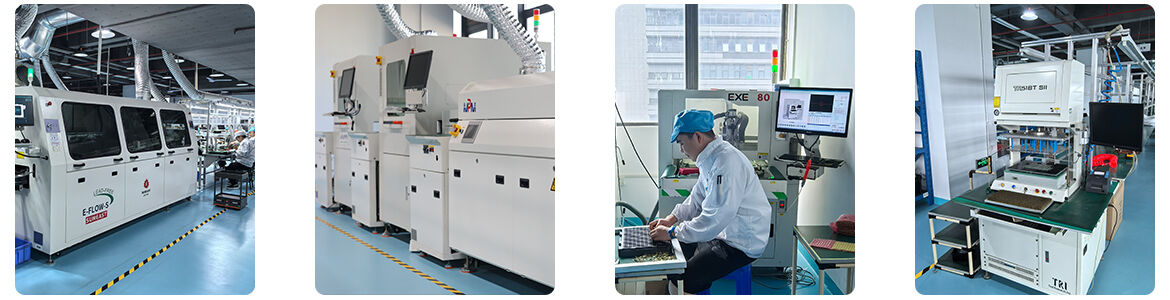
Manufacturing Capabilities
| PCB Manufacturing Capability | |||||
| ltem | Production capability | Min space for S/M to pad, to SMT | 0.075mm/0.1mm | Homogeneity of Plating Cu | z90% |
| Layer Count | 1~40 | Min space for legend to pad/ to SMT | 0.2mm/0.2mm | Accuracy of pattern to pattern | ±3mil(±0.075mm) |
| Production size(Min & Max) | 250mmx40mm/710mmx250mm | Surface treatment thickness for Ni/Au/Sn/OSP | 1~6um /0.05~0.76um /4~20um/ 1um | Accuracy of pattern to hole | ±4mil (±0.1mm ) |
| Copper thickness of lamination | 1/3 ~ 10z | Min size E- tested pad | 8 X 8mil | Min line width/space | 0.045 /0.045 |
| Product board thickness | 0.036~2.5mm | Min space between tested pads | 8mil | Etching tolerance | +20%0.02mm) |
| Auto-cutting accuracy | 0.1mm | Min dimention tolerance of outline (outside edge to circuit) | ±0.1mm | Cover layer alignment tolerance | ±6mil (±0.1 mm) |
| Drill size(Min/Max/hole sizetolerance) | 0.075mm/6.5mm/±0.025mm | Min dimention tolerance of outline | ±0.1mm | Excessive adhesive tolerancefor pressing C/L | 0.1mm |
| Warp&Twist | ≤0.5% | Min R corner radius of outline(inner filleted corner) | 0.2mm | Alignment tolerance forthermosetting S/M and UV S/M | ±0.3mm |
| maximum aspect Ratio(thickness/hole diameter) | 8:1 | Min space golden finger to outline | 0.075mm | Min S/M bridge | 0.1mm |