Introducció: Per què el muntatge SMT és l'opció preferida en l'electrònica moderna
El món de la fabricació d'electrònica ha viscut un canvi transformador durant les últimes dècades. Al centre d'aquesta revolució hi ha Tecnologia de Muntatge en Superfície (SMT) , un procés que ha impulsat la miniaturització de l'electrònica i ha assolit nivells de rendiment que abans eren inimaginables.
Principals motors de l'adopció del SMT
- Demanda de dispositius compactes: L'electrònica moderna—mòbils, rellotges intel·ligents, aparells auditius—requereix circuits densament empaquetats per oferir un alt rendiment en formats petits.
- Eficiència de la línia de muntatge: La necessitat de producció més ràpida, fiable i escalable ha dut als fabricants a optar pel muntatge automàtic de PCB.
- Funcionalitat millorada: La SMT permet la integració de més funcions per centímetre quadrat, revolucionant el disseny de PCB i ampliant les capacitats dels dispositius.
- Pressions de cost: La competència global i les expectatives dels consumidors respecte a tecnologia assequible han convertit la reducció de costos en la fabricació de PCB en una prioritat màxima.
Què és la tecnologia de muntatge en superfície (SMT)?
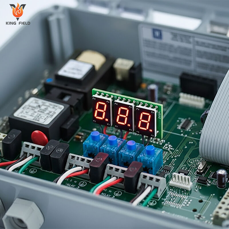
Tecnologia de Muntatge en Superfície (SMT) és un mètode modern utilitzat per muntar i soldar components electrònics directament sobre la superfície de circuitos impresos (PCB) . A diferència de les tècniques tradicionals, que es basaven en inserir les potes dels components a través de forats al PCB, la SMT permet col·locació directa, major automatització i una densitat de circuit excepcional , el qual beneficia significativament fabricació d'electrònics .
Context històric: del muntatge amb forats al muntatge superficial
A l' dècades del 1970 i 1980 , la fabricació d'electrònica estava dominada per Tecnologia de Forats Passants (THT) els components com ara resistències, condensadors i circuits integrats (IC) portaven cables que s'inserien manualment o mecànicament en forats perforats a les PCB. Aquest mètode, tot i ser robust, presentava diversos reptes:
- Intensiu en mà d'obra manual: Es requeria una mà d'obra significativa per a la inserció i soldadura.
- Miniaturització limitada: Els cables voluminosos i els forats limitaven fins a quin punt podia ser compacte el disseny d'una PCB.
- Producció més lenta: Productes complexos necessitaven molt de temps per al muntatge i la inspecció.
- Automatització restringida: L'automatització completa era difícil, cosa que augmentava les taxes d'error i els costos laborals.
|
|
Tecnologia de Forats Passants (THT)
|
Tecnologia de Muntatge en Superfície (SMT)
|
|
Muntatge de components
|
Conductors a través de forats perforats
|
Components col·locats directament sobre la superfície
|
|
Mida
|
Més grans, menys densos
|
Compactes, alta densitat
|
|
Nivell d'automatització
|
Baix a Moderat
|
Altament automatitzat
|
|
Velocitat de muntatge
|
Més lent
|
Molt ràpid
|
|
Flexibilitat en el Disseny
|
Limitat
|
Alta
|
La necessitat d'automatització i eficiència
A mesura que creixia la demanda de dispositius electrònics més petits, més eficients i més potents, els fabricants van buscar maneres d'incloure més circuits en taules més petites. Automatització en l'assemblatge de PCB es va convertir en una necessitat crítica.
- Les insercions es van convertir en un coll d'ampolla: Muntar components a través de forats—especialment a mesura que els dispositius es reduïen—ralentia la producció en massa.
- La densitat de components va arribar als límits físics: Els terminals i forats ocupaven un espai valuós a les plaques.
- La inspecció i reparació eren laborioses: Els processos manuals comprometien el rendiment i la capacitat de producció.
Aparició i dominança de la tecnologia SMT
Amb SMT , components—anomenats dispositius de muntatge superficial (SMD) —es col·loquen directament sobre les pastilles de la PCB. Sistemes automàtics màquines de col·locació automàtica posicionen aquests components amb precisió a velocitats molt elevades, seguits per soldadura per refluix per fixar-los.
Principals avantatges de l'aparició de la tecnologia SMT:
- Eliminació de forats perforats: Maximitza la superfície útil del PCB i permet dissenys més compactes.
- Muntatge automàtic ràpid: Productivitat molt més elevada i reducció d'errors humans.
- Components SMT adaptats al rendiment: Optimitzats per a altes freqüències, baix consum i paràsits mínims.
SMT vs. Mètodes tradicionals de muntatge (Through-Hole)
A mesura que ha evolucionat la fabricació d'electrònica, dues tècniques principals de muntatge de PCB han definit el panorama: Tecnologia de Forats Passants (THT) i Tecnologia de Muntatge en Superfície (SMT) comprendre les subtilitats, fortalezas i debilitats de tots dos mètodes és essencial per seleccionar l'enfocament adequat o la combinació adequada de mètodes per a una aplicació determinada.
Tecnologia de Forats Passants (THT): La referència en robustesa
Tecnologia de Forats Passants va ser l'eix de la indústria electrònica durant dècades. Aquí, components electrònics amb cables amb extrems lliures s'insereixen en forats prèviament perforats a les PCB i després es solden a les pastilles situades a la cara inferior de la placa. Aquesta tècnica ofereix algunes avantatges importants:
Fortaleses de l'assemblatge THT:
- Resistència mecànica: Els extrems fixats a través de la PCB proporcionen una gran integritat estructural, essencial per a components pesats o sotmesos a altes càrregues (per exemple, connectors d'alimentació, transformadors).
- Fiabilitat en entorns agressius: Particularment valorada en electrònica automotriu, aeroespacial i industrial, on hi ha preocupacions per vibracions, cicles tèrmics o xocs mecànics.
- Facilitat d'assemblatge manual i prototipatge: THT és adequat per a muntatges de tipus hobby, producció en petites sèries i escenaris que requereixen preses passants o connectors més grans.
Tecnologia d'Emmotlluratge en Superfície (SMT): El paradigma de la miniaturització
Tecnologia d'Emmotlluratge en Superfície s'ha convertit ràpidament en l'estàndard per a la fabricació moderna d'electrònica. En emmotllar els components directament sobre la superfície del PCB, la SMT elimina la necessitat de forats perforats, permetent millores revolucionàries:
Fortaleses de l'assemblatge SMT:
- Alta densitat de components: Permet dissenys de PCB extremadament compactes, essencials per a smartphones, implants mèdics i dispositius IoT.
- Automatització excepcional: Robòtics de presa i col·locació, forns de refusió d'alta velocitat i inspecció òptica automàtica (AOI) ofereixen velocitat, precisió i alts rendiments de producció.
- Eficiència més ràpida de la línia d'assemblatge: L'eliminació de la inserció manual i la soldadura en múltiples passos redueix els temps de producció.
- Rendiment elèctric superior: Camins conductors més curts i directes redueixen la inductància i la capacitància no desitjades, cosa que fa que la tecnologia SMT sigui ideal per a electrònica d'alta freqüència .
- Suport per a la miniaturització: Mides d'embalatge més petites recolzen la reducció contínua dels dispositius electrònics.
- Dissipació de potència més baixa: Els resistors i condensadors SMT solen tenir classificacions de potència reduïdes i una millor gestió tèrmica degut a les connexions més curtes i embalatges optimitzats.
Taula comparativa de referència ràpida
|
Criteris
|
Tecnologia de Forats Passants (THT)
|
Tecnologia de Muntatge en Superfície (SMT)
|
|
Mètode de muntatge
|
Conductors a través de forats perforats
|
Components a la superfície del circuit imprès
|
|
Mida del component
|
Més gran, més voluminós
|
Petit, compacte
|
|
Densitat de circuit
|
Baix
|
Alta
|
|
Velocitat de muntatge
|
Lentament
|
Ràpid (altament automatitzat)
|
|
Força Mecànica
|
Alt (per a components grans)
|
Limitat (millor per a dispositius petits)
|
|
Rendiment elèctric
|
Limitat a alta freqüència
|
Superior per a alta freqüència
|
|
Automatització
|
Moderat a difícil
|
Extensiva; fàcilment automatitzable
|
|
Prototipat
|
Fàcil
|
Més complicat
|
|
Casos d'ús típics
|
Industrial, Aeroespacial, Automoció (parts de potència)
|
Consumidor, Mòbil, IoT, Mèdica
|
El cas de l'assemblatge de PCB de tecnologia mixta
Cada cop més, l'assemblatge de PCB de tecnologia mixta —que combina tant SMT com THT—ofereix el millor dels dos mons:
- Ús SMT per a senyals d'alta densitat i alta velocitat i àrees compactes.
- Ús THT per a components que requereixen resistència mecànica o gestió d'alta corrent.
Avantatges principals de l'assemblatge SMT en la fabricació electrònica
La transició cap a la Tecnologia de Muntatge en Superfície (SMT) ha inaugurat una nova era per a la indústria electrònica. L'assemblatge SMT aporta una àmplia gamma d'avantatges, transformant gairebé totes les fases del Fabricació de PCB , des de l'eficiència del disseny i la densitat de components fins a l'efectivitat econòmica i la fiabilitat. Analitzem a fons aquests beneficis principals i veiem per què l'assemblatge SMT és ara l'estàndard en la fabricació electrònica moderna.
1. Major eficiència d'assemblatge i automatització
Una de les avantatges més transformadores de Muntatge SMT és la capacitat d’aprofitar l’automatització per assolir una velocitat i consistència sense precedents:
- Col·locació automàtica de components: Utilitzant tecnologia avançada màquines de col·locació automàtica , milers de components de muntatge superficial poden col·locar-se amb precisió sobre una PCB en pocs minuts.
- Procés de soldadura racionalitzat: La tècnica de soldadura per refusió permet soldar tots els circuits alhora, augmentant encara més el rendiment i el rendiment útil.
- Reducció dels errors humans: L’automatització a gran escala minimitza el risc de defectes de soldadura, components desalineats o orientació incorrecta.
2. Disseny de PCB compacte i major densitat de components
Components SMT són dràsticament més petits que els seus homòlegs de forat passant. Les seves petites empremtes permeten als enginyers dissenyar circuits d'alta densitat , permetent una funcionalitat més complexa en un espai mínim a la placa.
Beneficis de l'alta densitat de components:
- Miniaturització de l'electrònica: Els smartphones, dispositius portàtils i dispositius IoT d'avui són possibles només gràcies a muntatges SMT compactes.
- Suport per PCB de múltiples capes: La tecnologia SMT permet empilaments de múltiples capes sense problemes, oferint encaminaments avançats per a dissenys complexos.
- Flexibilitat de disseny millorada: Els paquets SMT més petits (com el 0402 o el 0201 per a resistències/condensadors) permeten als dissenyadors incloure una gamma més àmplia de funcions o velocitats més altes en espais reduïts.
3. Potències nominals inferiors i un rendiment millorat
Resistències i condensadors SMT normalment ofereixen una menor dissipació de potència deguda a les seves mides reduïdes i longituds de conductor optimitzades. A més, les configuracions de muntatge superficial permeten:
- Menor inductància i capacitància en el camí elèctric: Les connexions més curtes redueixen els elements paràsits, cosa que fa que el SMT sigui ideal per a circuits d'alta freqüència i alta velocitat.
- Millor rendiment tèrmic: Eficient gestió tèrmica i una major resistència tèrmica en els paquets SMT moderns redueixen el risc de sobrecalentament.
4. Reducció de costos en la fabricació de PCB
L'eficiència de cost és un dels principals motors per l'adopció del SMT, amb impacte tant en fabricants de petita escala com en grans volums:
- Menys forats perforats: El muntatge directe a la superfície elimina passos de perforació cars i que consumeixen temps.
- Costos de materials reduïts: Els paquets més petits signifiquen menys material per component.
- Costos laborals més baixos: L'automatització optimitza el Procés de muntatge de PCB , reduint significativament els requisits de mà d'obra manual.
- Qualitat constant: Menys defectes i treballs de revisió porten a taxes de rendiment més altes en general.
Taula: Comparació estimada de costos (valors típics)
|
Mètode de muntatge
|
Cost de mà d'obra per placa
|
Cost del component
|
Cost de l'equipament (per unitat, amortitzat)
|
Taxa de rendiment
|
|
THT (Manual)
|
Alta
|
Estàndard
|
Baix
|
92%
|
|
SMT (Automatitzat)
|
Molt baix
|
Menor
|
Moderat/Alt
|
98%
|
5. Fiabilitat millorada i rendiment optimitzat
- Juntes de soldadura uniformes: Els processos automatitzats de refusió creen connexions consistents i fiables que tenen menys probabilitats de fallar que les juntes soldades a mà.
- Característiques de freqüència més elevades millorades: Els camins superficials curts del SMT milloren la integritat del senyal a alta freqüència i redueixen la interferència electromagnètica.
- Compatibilitat amb soldadures sense plom: El SMT s’adapta més fàcilment a soldadura sense plom normes, que recolzen el compliment ambiental i regulador.
6. Compatibilitat completa amb muntatges mixtes i híbrids
Encara que la tecnologia SMT hagi substituït en gran mesura la de forats passants en l'electrònica de consum, una de les seves qualitats menys comentades és la coexistència amb circuits impresos de forats passants en muntatges PCB híbrids o de tecnologia mixta . Els fabricants poden optimitzar cada disseny utilitzant el millor dels dos mons; per exemple, combinant microcontroladors de muntatge superficial amb connectors de forats passants per obtenir un millor maneig de potència i una major durabilitat física.
7. Escalabilitat incomparable per a la producció massiva
Un cop el disseny d'un circuit imprès està preparat, Línies d'assemblatge SMT poden escalar-se gairebé infinitament, servint tant per a la producció massiva per a electrònica de Consum i els exigents estàndards de qualitat de mèdic i pCB aerospacial fabricació.
Clau de les conclusions:
- Òptim per a grans volums de producció.
- Adequat per a plafons complexos, multilayer i compactes.
- Proporciona l'agilitat necessària per als mercats electrònics competitius.
8. Fiabilitat i consistència millorades amb el temps
Perquè l'assemblatge SMT allibera el procés de la majoria d'intervencions humans, Circuits SMT ofereixen una vida útil més llarga, una major consistència i una fiabilitat general superior. Acompanyats de funcions integrades d'autocomprovació i inspecció òptica automàtica (AOI) , les taxes de fallada es minimitzen significativament.
Avantatges de la SMT: Llista de referència ràpida
- Disseny de circuits d'alta densitat
- Automatització i escalabilitat sense interrupcions
- Muntatge més ràpid i temps reduït fins al mercat
- Costos totals més baixos de fabricació i mà d'obra
- Rendiment superior en freqüències altes i senyals
- Disseny de productes més petits, lleugers i integrats
- Respectuós amb el medi ambient, compatible amb estàndards lliures de plom
Explorant components i dispositius SMT
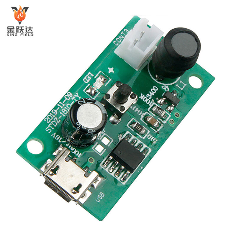
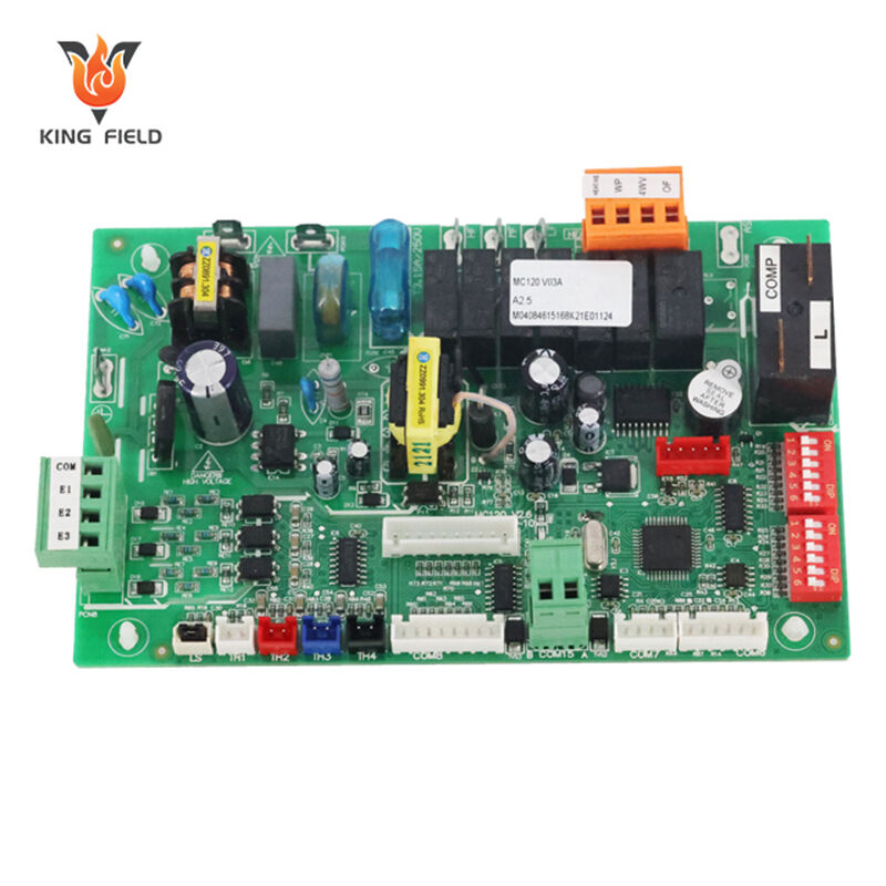
La tecnologia de muntatge en superfície (SMT) ha permès el desenvolupament d'una àmplia gamma de components electrònics especialitzats dissenyats per a muntatges PCB altament automatitzats i d'alta densitat. Les seves característiques físiques i envasats únics han contribuït directament a la miniaturització de l'electrònica i al compliment dels requisits de disseny complexos en dispositius moderns. En aquesta secció, analitzarem detalladament els tipus de Components SMT , els seus estils d'envasat i com difereixen dels homòlegs tradicionals de forat passant.
Components SMT vs. Components de forat passant
La diferència fonamental entre els components de muntatge en superfície i els de forat passant rau en la manera com es connecten a la placa de circuit imprès (PCB):
- Components through-hole tenen cables amb extrems inserits en forats metallsats i soldats al costat oposat.
- Components SMT (o dispositius de muntatge superficial, SMD) tenen terminacions metàl·liques o extrems que es col·loquen directament sobre les pastilles de soldadura de la PCB i s'uneixen mitjançant soldadura per refús.
Diferències principals
|
Característica
|
Components SMT
|
Components through-hole
|
|
Mètode de muntatge
|
A la superfície del PCB
|
A través de forats PCB
|
|
Mida del paquet
|
Molt petit, compacte
|
Típicament més gran
|
|
Muntatge
|
Possible completament automàtic
|
Principalment manual/semi-automàtic
|
|
Rendiment del senyal
|
Baixos paràsits, alta velocitat
|
Inductància/capacitància més elevada
|
|
Aplicació
|
Alta densitat/compacte
|
Es requereix resistència mecànica
|
Principals tipus de paquets SMT
1. Components passius: Resistors i condensadors
Els resistors i condensadors SMT venen en paquets estandarditzats i miniaturitzats dissenyats per facilitar la seva identificació automàtica per part dels equips de muntatge automatitzats:
|
Codi de mida SMT comú
|
Mida mètrica (mm)
|
Casos d'ús típics
|
|
1206
|
3,2 × 1,6
|
Potència, placa menys densa
|
|
0805
|
2,0 × 1,3
|
Disseny de densitat mixta
|
|
0603
|
1,6 × 0,8
|
Electrònica de Consum
|
|
0402
|
1,0 × 0,5
|
D'alta densitat, mòbil
|
|
0201
|
0,6 × 0,3
|
Ultracompacte, IoT
|
2. Circuits Integrats (CI)
La tecnologia SMT ha permès l'empaquetat i muntatge de CI molt complexos, com ara microcontroladors, FPGAs i xips de memòria.
Paquets SMT populars de CI:
|
Tipus d'embalatge
|
Abreviatura
|
Rang de nombre de pins
|
Amplada típica (mm)
|
Aplicació d'exemple
|
|
Circuit Integrat d'Empra Reduïda
|
SOIC
|
8–50
|
3.9–12.8
|
Lògica, controladors
|
|
Paquet pla quadrat
|
QFP
|
32–256
|
9–32
|
Microcontrolador, DSP
|
|
Matriu de boles
|
BGA
|
32–1000+
|
5–35
|
UCPs, FPGAs
|
|
Paquet a escala de xip
|
CSP
|
8–100+
|
2–10
|
Processadors mòbils
|
3. Semiconductors discrets: Transistors i díodes
Els semiconductors discrets ara es subministren principalment en petits paquets de plàstic per a muntatge superficial, millorant tant l'automatització com l'eficiència del circuit imprès.
Paquets habituals:
- SOT-23, SOT-223: Ampliament utilitzats per a transistors bipolars, FETs i reguladors de tensió.
- SOD, MELF: Per a díodes i components passius especialitzats.
4. Altres tipus de components SMT
- Inductors: Disponibles com xips petits o paquets bobinats per a circuits de RF i d'alimentació.
- Connectors: Fins i tot alguns connectors miniaturitzats ara es presenten en variants híbrides o totalment SMT, optimitzats per a la col·locació automàtica però que encara ofereixen una gran robustesa mecànica.
- Oscil·ladors i cristalls: Les variants SMT simplifiquen la integració de temporitzacions d'alta velocitat.
Orientació i col·locació dels components SMT
Alta velocitat màquines de col·locació automàtica llegeixen els alimentadors de components, orienten cada peça amb precisió i la col·loquen sobre pads amb pasta de soldar. Aquesta precisió assegura una taxa màxima de rendiment de PCB i repetibilitat, minimitzant els riscos associats a la manipulació humana.
Consideracions habituals de col·locació
- Orientació del component: Assegura que el pin 1 o les marques de polaritat coincideixin amb el disseny del PCB: essencial per a circuits integrats i condensadors polaritzats.
- Resistència tèrmica: Els components SMT estan dissenyats per a altes temperatures cicle tèrmic i pot suportar la calor intensa de forns de refluència .
- Codificació del component: Les marques clares i els codis estandarditzats ajuden els sistemes d'inspecció òptica automàtica (AOI) a verificar la col·locació correcta.
Taula: Resum de referència de paquets SMT
|
Categoria
|
Exemples (Paquet)
|
Interval de mida típic
|
Mètode de muntatge
|
|
Resistors
|
0201, 0402, 0603
|
0,6 mm–1,6 mm
|
Automatitzat, pasta de soldadura i refluix
|
|
Condensadors
|
0402, 0805, 1206
|
1,0 mm–3,2 mm
|
Automatitzat, pasta de soldadura i refluix
|
|
ICs
|
SOIC, QFP, BGA, CSP
|
3,9 mm – 35 mm
|
Automatitzat, pasta de soldadura i refluix
|
|
Transistors
|
SOT-23, SOT-223
|
1,2 mm – 6 mm
|
Automatitzat, pasta de soldadura i refluix
|
|
Díodes
|
SOD, MELF
|
1,0 mm – 5 mm
|
Automatitzat, pasta de soldadura i refluix
|
Dins del procés de muntatge SMT: pas a pas
Les Procés de muntatge SMT és una sèrie sofisticada i altament automatitzada de passos que integra precisió mecànica, química i visió per ordinador per produir de manera fiable circuitos impresos (PCB) . Tot el flux de treball està dissenyat per maximitzar la fiabilitat, la integritat del senyal i el rendiment de producció, convertint-lo en el nucli del modern fabricació d'electrònics . A continuació, desglossarem cada fase principal, explorant les maquinàries avançades, els controls de procés i les avantatges SMT resultants.
1. Aplicació de pasta de soldar
El viatge d'una placa SMT comença amb l' aplicació de la pasta de soldar sobre els pads del PCB nu.
Pasta de soldar és una barreja de partícules minúscules de solda i flux. Serveix alhora d'adhesiu per mantenir els components durant la col·locació i de solda real per a la unió permanent durant el procés de refluït.
Passos clau:
- A estenedor d'acer inoxidable —tallat a mida per encaixar amb la distribució dels pads— es col·loca sobre el PCB.
- Impressores automàtiques de serigrafia apliquen pasta de soldadura a través de les obertures del motlle, recobrint cada pad amb un dipòsit precís.
- Màquines avançades verifiquen el volum i la ubicació de cada dipòsit de pasta mitjançant inspecció de pasta de soldadura (SPI) sistemes.
2. Col·locació de components (tecnologia Pick-and-Place)
A continuació, màquines d'última generació màquines de col·locació automàtica entren en acció:
- Alimentadors de components : Cada component SMD (dispositiu de muntatge superficial) s'inseriex a la màquina mitjançant bobines, tubs o plataformes.
- Sistemes de visió : Capçals guiats per càmera agafen els components mitjançant aspiració pneumàtica, verifiquen l'orientació i asseguren la mida i el tipus.
- Col·locació a alta velocitat : El col·locació automàtica el cap col·loca cada component sobre la PCB acabada d’engomar a velocitats de desenes de milers de col·locacions per hora.
3. Soldadura per reflujo: El nucli de la unió SMT
Potser la característica més important i única del muntatge SMT, soldadura per refluix és on les unions temporals de la pasta de soldadura es converteixen en connexions elèctriques i mecàniques fiables i permanents.
Fases del procés en la soldadura per reflujo:
|
Fase
|
Rango de temperatura
|
Finalitat principal
|
Durada
|
|
Zona de preescalfament
|
130–160°C
|
Escalfament gradual de la PCB, activació del flux
|
60–120 seg
|
|
Zona de manteniment
|
160–200°C
|
Evaporar volàtils, mullar solda
|
90–120 seg
|
|
Zona de reflux
|
220–250°C
|
Fondre solda, formar unions
|
30–60 seg
|
|
Zona de refredament
|
~150°C → ambient
|
Solidificar solda, estabilitzar unions
|
60–120 seg
|
- Perfils tèrmics estan optimitzats per al tipus de component i PCB, evitant danys als paquets SMT sensibles.
- Les plaques passen a través de forns de refusió automàtics amb gradients tèrmics precisament controlats.
4. Inspecció òptica automàtica (AOI) i comprovacions de qualitat
Un cop sortides del forn de refusió, les PCB es dirigeixen ràpidament a inspecció òptica automàtica (AOI) estacions:
- L'AOI utilitza càmeres d'alta resolució per comparar cada placa muntada amb referències prèviament programades, verificant components desplaçats, absents o mal orientats així com la integritat de les unions de soldadura.
- Els sistemes AOI avançats analitzen milers de característiques per placa en segons, detectant defectes invisibles a ull nu.
- En moltes línies, Inspecció amb raigs X s'utilitza per a paquets altament complexos (com ara BGAs) per identificar defectes ocults com buits, soldadura insuficient o curtcircuits sota l'embalatge.
Passos addicionals de qualitat
- Proves Funcionals: En muntatges PCB d'alt valor o crítics per a la seguretat, estacions de prova funcionals en línia o al final de la línia validen el rendiment en condicions operatives simulades.
- Revisió manual: De tant en tant, les plaques detectades són revisades per tècnics qualificats per a la reparació o accions correctores.
5. Netegesa final i preparació
Fins i tot la soldadura sense plom i de procés net pot deixar residus microscòpics. En plaques d'alta fiabilitat (mèdiques, automotriu, aerospacial), sistemes automàtics de rentat i assecat eliminen tot el flux residual o partícules restants per prevenir la corrosió i fuites de senyal.
Flux del procés de muntatge SMT — Taula resum
|
Pas
|
Equip implicat
|
Nivell d'automatització
|
Control de qualitat
|
|
Aplicació de pasta de soldadura
|
Impressora de serigrafia, SPI
|
Totalment automatitzat
|
Inspecció de pasta de soldadura (SPI)
|
|
Col·locació de components
|
Màquina de col·locació automàtica
|
Totalment automatitzat
|
Precisió amb guia visual
|
|
Soldadura per refluix
|
Forn de refluix
|
Totalment automatitzat
|
Validació del perfil tèrmic
|
|
Inspecció i proves
|
AOI, raigs X, testers de circuit en línia
|
Principalment automatitzat
|
Detecció de defectes, proves de rendiment
|
|
Neteja/Acabat
|
Estació de rentat/assecat
|
Parcialment automatitzat
|
Prova de contaminació iònica (si és necessària)
|
Estudi de cas: Ampliació per a la producció moderna
Global electrònica de Consum utilitza línies SMT per produir PCBs de telèfons intel·ligents. Cada línia:
- Funciona 24/7 amb mínima intervenció humana
- Assoleix més del 99,9% de taxa de rendiment en més de 10.000 plafons per torn
- Detecta i resol automàticament problemes en temps real, assegurant una qualitat uniforme
El paper de l'expertesa humana
Tot i que el muntatge SMT fa èmfasi en l'automatització, els enginyers i tècnics humans són essencials per:
- Programar sistemes de col·locació i inspecció
- Resoldre errors de procés inesperats
- Dissenyar nous circuits per a facilitat de fabricació (vegeu DFM, secció següent)
Resum
Les Procés de muntatge PCB SMT exemplifica com la sinergia entre eines avançades, controls rigorosos del procés i una supervisió experta condueix a soldadura de precisió, taxes de rendiment extremadament altes i una fiabilitat excepcional del producte —atributs que defineixen la millor fabricació d'electrònica actual.
L'avantatge dels PCB de tecnologia mixta (SMT + THT)
Mentre Tecnologia de Muntatge en Superfície (SMT) domina el panorama de la fabricació d'electrònica moderna, Tecnologia de Forats Passants (THT) continua sent indispensable per a nombroses aplicacions d’alta fiabilitat o alta tensió. Aprofitant les fortaleses de tots dos, els enginyers han desenvolupat l'assemblatge de PCB de tecnologia mixta —un enfocament híbrid que obre noves alçades de flexibilitat de disseny, fiabilitat i rendiment.
Què és l'assemblatge de PCB de tecnologia mixta?
L'assemblatge de PCB de tecnologia mixta implica combinar estratègicament Components SMT i components tradicionals THT en una sola placa de circuit. Aquest mètode permet als fabricants aprofitar les avantatges de la miniaturització, col·locació automàtica i estalvi de costos de la tecnologia SMT mantenint alhora la robustesa mecànica i la capacitat de gestió de potència dels components THT.
Principals Vantatges:
- Optimitza l'espai i el rendiment: La lògica densa i les línies de senyal d'alta velocitat utilitzen SMT, mentre que les càrregues pesades i els connectors aprofiten THT.
- Millora la fiabilitat de la placa: Els suports mecànics crítics (connectors d'alimentació, relés) suporten vibracions, impactes i esforços repetits.
- Permet la multifuncionalitat: Suporta dissenys complexos de PCB multicapa per a aplicacions avançades en automoció, aerospacial, industrial i mèdica.
Flux de treball d'un muntatge de PCB de tecnologia mixta
Procés d'assemblatge mixt pas a pas
|
Pas
|
Procés SMT
|
Procés THT
|
Nivell d'automatització
|
|
1
|
Impressió de pasta de soldar (per a pads SMT)
|
Forats perforats, pads recoberts
|
Automatitzat (SMT), Semiautomatitzat (THT)
|
|
2
|
Col·locació automàtica de components SMT
|
|
Altament automatitzat
|
|
3
|
Soldatge per refluix (tots els SMD)
|
|
Automatitzat
|
|
4
|
Inspecció òptica automàtica (AOI)
|
|
Automatitzat
|
|
5
|
Girar la placa (si és doble cara) i repetir els passos 1–4
|
|
Automatitzat
|
|
6
|
Inserció de components THT
|
Inserció manual o robòtica de components de forat passant
|
Semi-automatitzat a Automatitzat (Robot/Inseridor en línia)
|
|
7
|
Soldadura THT (Onda/Selectiva/Manual)
|
Flux de solda fos per completar les connexions THT
|
De semi a totalment automatitzat
|
|
8
|
Neteja, inspecció final i proves
|
Inspecció completa de tot el muntatge
|
Combinat
|
Soldadura avançada per a muntatges híbrids
- Soldadura per ona: Eficient per a grans volums però pot provocar estrès tèrmic en components sensibles.
- Soldadura selectiva: La calor dirigida redueix el risc en dissenys sensibles o densos, essencial per a circuits complexos d'automoció o defensa.
- Tècnica Pin-in-Paste: Els pins THT o les potes s'insereixen temporalment en la pasta de soldadura SMT i després es solden durant la fase de reflujo, ideal per a produccions de baix volum, especialitzades o prototips.
Aplicacions del món real i casos pràctics
PCB per a automoció i indústria
- Els controladors del motor utilitzen microcontroladors i lògica SMT juntament amb connectors THT i relés d'alta potència.
- Els sistemes de control de processos industrials utilitzen SMT per a camins de senyal ràpids i compactes, però THT per a blocs de terminals grans.
Dispositius Mèdics
- SMT permet un processament dens de senyals en monitors portàtils, mentre que els connectors robustos THT asseguren estabilitat en entorns d'alta fiabilitat (per exemple, equips hospitalaris o dispositius implantables).
Aeroespacial i Defensa
- Les plaques de circuit d'avionics utilitzen SMT per reduir el pes i augmentar la densitat lògica, reservant el THT per a connectors crítics que han de suportar vibracions, xocs i múltiples connexions.
Estudi de Cas: Un PCB de ventilador mèdic combina xips de processament analògics/digitals SMT i passius miniaturitzats amb connectors THT capaços de suportar múltiples esterilitzacions i esforços físics, maximitzant tant la densitat del circuit com la seguretat.
Aclariment de termes: Tecnologia mixta vs. Senyal mixta
- Tecnologia mixta PCB: Utilitza components SMT i THT per assolir un disseny òptim, fabricabilitat i fiabilitat.
- PCB de senyal mixta: Integra circuits analògics i digitals, sovint requerint consideracions cuidadoses en disseny físic i disposició, però sense estar lligat als mètodes de muntatge.
La síntesi estratègica: Per què els enginyers de disseny adopten PCB híbrids
- Eficiència de disseny: Cada component es selecciona i munta allà on té millor rendiment i major durabilitat.
- Agilitat en la fabricació: Els dissenyadors poden adaptar ràpidament plataformes existents a nous requisits canviant només algunes peces THT o SMT.
- Futur-proofing: A mesura que els paquets SMT i els suports THT continuen evolucionant, les PCB de tecnologia mixta romandran adaptables tant per al maquinari heretat com per a funcionalitats d'avantguarda.
Disseny per a la Fabricació (DFM) en Montatge SMT i Mixt
El camí des del concepte fins a la PCB perfectament produïda en sèrie està ple de decisions intrincades. Disseny per a la Fabricació (DFM) és el conjunt de principis i pràctiques que asseguren que un disseny de PCB estigui optimitzat per a un muntatge sense problemes i econòmic—especialment important per a plafons híbrids que incorporen tant Tecnologia de Muntatge en Superfície (SMT) i Tecnologia de Forats Passants (THT) al món accelerat de fabricació d'electrònics , el DFM adequat tanca la bretxa entre un disseny d'alt rendiment i una producció fiable.
Els Fonaments del DFM en el Muntatge de PCB
El DFM comença en les primeres etapes del procés de distribució del PCB. Els seus objectius principals són:
- Reduir el risc d'errors durant el muntatge.
- Minimitzar els costos de fabricació i el temps de cicle.
- Assegurar un rendiment robust i fiable del circuit impregnat.
- Millorar automatització en l'assemblatge de PCB .
- Optimitzar les proves i l'assegurament de qualitat a posteriori.
1. Disposició del PCB, espaiat i regles crítiques de DFM
Una disposició adequada assegura que cada component SMT i THT es pugui col·locar, soldar i inspeccionar sense risc de defectes o interferències:
- Espaiat mínim de pads: Mantenir una distància suficient entre els pads SMT per evitar ponts de soldadura i permetre la precisió de SPI/AOI.
- Separació al voltant dels forats: Per a muntatges mixtos, ha d'haver-hi un espaiat adequat entre els forats passants i els pads SMT adjacents o pistes, tenint en compte la possible dissipació tèrmica durant la soldadura per ona o manual.
- Amplària de Traça i Mida de Vies: Equilibra les necessitats de transport de corrent amb l'espai disponible a la placa, especialment complicat en PCBs densos de múltiples capes.
- Agrupació de Components: Agrupa components similars (per funció o mida) per optimitzar les operacions de col·locació i inspecció.
Taula de Regles Pràctiques de DFM
|
Paràmetre
|
SMT Mínim
|
THT Mínim
|
Recomanació d'Assemblatge Mixt
|
|
Espaiat entre Pads
|
≥ 0,20 mm
|
N/A
|
0,20 mm (SMT a THT: ≥ 0,50 mm)
|
|
Separació traça-pastilla
|
≥ 0,10 mm
|
≥ 0,20 mm
|
0.20 mm
|
|
Separació forat-pastilla
|
N/A
|
≥ 0,25 mm
|
≥ 0,50 mm (si és proper a SMT)
|
|
Vora del component a vora
|
≥ 0,25 mm
|
≥ 0,50 mm
|
≥ 0,60 mm (per accés AOI)
|
2. Estratègies de gestió tèrmica
Dissenyos SMT d'alta densitat de components i placa híbrides amb components THT per a maneig de potència requereixen controls tèrmics intel·ligents:
- Vies tèrmiques: Orificis revestits de coure col·locats estratègicament transfereixen l'excés de calor des dels paquets SMT (com BGAs o MOSFETs de potència) cap a capes interiors o oposades del circuit imprès.
- Abocament de coure i plans: Rastes més amples i àrees grans de coure distribueixen la calor, millorant la dissipació i el blindatge contra interferències electromagnètiques (EMI).
- Dissipadors tèrmics i pantalles: Per a components THT crítics o d’alta potència, integriu dissipadors tèrmics mecànics o pantalles al muntatge mecànic del circuit o considereu la dissipació tèrmica amb component sobre el circuit.
- Disseny de pads per a refluït: Per a dispositius SMD grans o sensibles a la calor, formes especialitzades de pads gestionen el perfil de calefacció/refredament i asseguren una soldadura uniforme.
4. Màscara de soldadura i serigrafia
- Màscara de soldar: Les màscares són essencials per evitar ponts de soldadura en pads SMT de pas fi i proporcionen contrast de color per a inspecció automàtica/visual.
- Serigrafia: Les marques adequades redueixen confusions en el muntatge manual, ajuden a l'AOI i agilitzen la reparació o substitució de components durant les proves i reparacions del PCB.
5. Proveïment i disponibilitat de components
Un PCB ben dissenyat només és fabricable si els components estan disponibles i els terminis d'entrega coincideixen amb les necessitats de producció:
- Llistes de components preferits: Els dissenyadors haurien d’utilitzar paquets SMT i THT estàndard i àmpliament disponibles per minimitzar els riscos d’aprovisionament.
- Components alternatius: Sempre cal especificar fonts alternatives per a components claus per evitar retards.
6. Accessibilitat a proves i inspeccions
- Punts de prova: Incloure pads o capçalers accessibles per a proves en circuit i funcionals.
- Disseny preparat per a AOI: Assegureu un espai suficient per als angles de la càmera, especialment al voltant d'àrees densament col·locades i de tecnologia mixta.
Automatització i inspecció avançades en la fabricació de PCB
Com Tecnologia de Muntatge en Superfície (SMT) ha madurat, modern Fabricació de PCB els entorns s'han transformat en fàbriques intel·ligents d'alta velocitat basades en dades. Automatització en l'assemblatge de PCB maximitza el volum de producció, redueix els errors humans i assegura una consistència extraordinària. Al mateix temps, les tecnologies d'inspecció automàtiques garanteixen la qualitat, fiabilitat i conformitat fins i tot per a les taules més complexes. Aquí, descobrirem les funcions essencials de l'automatització i la inspecció durant tot el cicle de muntatge SMT i de tecnologia mixta.
1. La funció de l'automatització en el muntatge SMT
L'automatització és l'eina fonamental de la fabricació avançada de PCB, ja que permet assolir una escala i precisió que el muntatge manual simplement no pot igualar.
Processos automatitzats clau:
-
Impressió de pasta de soldar:
- Les impressores automàtiques asseguren que cada calaix rebi la quantitat i el patró exactes de pasta de soldar. Això redueix els ponts o el tombament i permet dissenys miniaturitzats.
-
Tecnologia Pick-and-Place:
- Amb velocitats superiors a 60.000 col·locacions per hora, aquestes màquines llegueixen fitxers CAD, seleccionen components, els giren i posicionen amb precisió, i asseguren que l'orientació i el tipus de component siguin correctes.
-
Integració de cintes transportadores:
- Els circuits es desplacen sense interrupcions entre les diferents fases del procés: impressió serigràfica, col·locació, refluït i inspecció, minimitzant la manipulació humana i el risc de contaminació.
-
Forns de refluït:
- El perfilatge automàtic de temperatura assegura unions de soldadura consistents per a cada placa, independentment de la seva complexitat o combinació de components.
2. Inspecció automàtica: Assegurant la qualitat a gran escala
La inspecció és igual d'important que la col·locació o la soldadura. Avui en dia, la inspecció automàtica multinivell és estàndard:
a. Inspecció de pasta de soldar (SPI)
- Inspecciona cada depòsit de soldadura després de la impressió per verificar-ne el volum, àrea i alçada.
- Detecta problemes abans que es col·loquin components costosos.
b. Inspecció òptica automàtica (AOI)
- Utilitza imatges d'alta resolució i algorismes de reconeixement de patrons.
- Comprova si manquen components, estan mal alineats o tenen una orientació incorrecta.
- Inspecciona les unions de soldadura per detectar ponts, soldadura insuficient i tombstones (efecte tombstone).
- Pot implementar-se després de la col·locació i/o després de la soldadura per refluït.
c. Inspecció per raigs X (AXI)
- Essencial per a paquets amb unions ocultes com BGAs, QFNs i ICs complexos.
- Revela fallades internes en les connexions, buits i curtcircuits invisibles per a l'AOI.
d. Proves en circuit i funcionals
- Utilitza sondes elèctriques per validar la continuïtat, la resistència i el valor dels components.
- Els testers funcionals simulen el funcionament real del dispositiu per a una verificació de nivell superior.
3. Integració d'instal·lacions intel·ligents i dades en temps real
L'ascens del Industria 4.0 les tecnologies fan que actualment la majoria de línies SMT d'alta gamma recullin i analitzin dades detallades del procés:
- Anàlisi de rendiment: Mètriques en temps real sobre la qualitat de la pasta de soldar, la precisió de col·locació i els resultats d'inspecció identifiquen tendències o defectes emergents abans que afectin el rendiment.
- Retroalimentació del procés: Les màquines poden autocorregir-se o alertar els operadors sobre canvis en les condicions (per exemple, errors de recollida, fallades de les toveres).
- Traçabilitat: Els números de sèrie i els codis de barres 2D a cada PCB registren cada pas del procés i cada estació d'inspecció, donant suport a l'anàlisi de fallades i al compliment normatiu en sectors com l'automoció i l'aeroespacial.
Taula: Tecnologies clau d'inspecció automàtica i beneficis
|
Tipus d'inspecció
|
Funció Principal
|
Defectes típics detectats
|
Nivell d'automatització
|
|
Inspecció de pasta de soldadura (SPI)
|
Verificar volum/posició de la pasta
|
Soldadura insuficient/excessiva
|
Totalment automatitzat
|
|
Inspecció òptica automàtica (AOI)
|
Comprovació visual dels components i unions
|
Desalineació, ponts, peces absents
|
Totalment automatitzat
|
|
Inspecció per raigs X (AXI)
|
Imatges internes de les unions
|
Avaries en BGA, buits, curtcircuits enterrats
|
Principalment automatitzat
|
|
Prova en circuit/funcional
|
Prova elèctrica/operativa
|
Obertures, curtcircuits, valors incorrectes, avaries
|
Semiautomatitzat
|
4. Costos més baixos, rendiments més alts, consistència excepcional
- Reducció de la reprocessat: La detecció precoç redueix dràsticament les taxes de defectes després del muntatge.
- Cicles de producció més curts: Les inspeccions automàtiques permeten que les línies funcionin més temps, amb només les plàques realment defectuoses que requereixen intervenció humana.
- Fiabilitat superior: Controles automàtics rigurosos asseguren que les plàques compleixin o superin les especificacions del client en electrònica industrial, automotriu o mèdica.
5. El futur: aprenentatge automàtic i manteniment predictiu
Alguns dels fabricants més destacats estan implementant algorismes d'aprenentatge automàtic per analitzar desenes de milers d'imatges de control de processos i inspecció, preveient el desgast dels alimentadors de components, problemes en les plantilles o defectes subtils abans que es produeixin avaries greus. Això es tradueix en:
- Estratègies de zero defectes per a aplicacions crítiques.
- Una disponibilitat gairebé perfecta, fins i tot en instal·lacions de PCBA d'alta varietat i alt volum.
Consideracions econòmiques i assegurament de la qualitat
L'impuls cap a la innovació, la miniaturització i la fiabilitat en l'electrònica seria insostenible sense un marc econòmic sòlid i un rigorós assegurança de qualitat . La tecnologia d'instal·lació superficial (SMT) i els muntatges de PCB de tecnologia mixta afecten dramàticament tant el costos de producció i qualitat del producte , fent que aquests factors siguin essencials per a les empreses que volen mantenir-se competitives en la fabricació electrònica global.
1. Anàlisi de costos: SMT, THT i muntatge mixt
Un dels factors més importants que impulsen l'adopció de SMT—i la progressiva substitució de la tecnologia tradicional Tecnologia de Forats Passants (THT) per a la majoria d'aplicacions—és el notable eficiència en Costos que aporta tant a grans com a mitjanes sèries de producció.
Factors clau de cost:
|
Factor
|
Muntatge SMT
|
Muntatge en forat passant
|
PCB de tecnologia mixta
|
|
Cost de mà d'obra
|
Molt baix (automatitzat)
|
Alt (manual/semiautomàtic)
|
Mitjà
|
|
Aprofitament del material
|
Alta densitat, menys residus
|
Densitat inferior, més residus
|
Variable
|
|
Inversió en equipament
|
Alt inicial, baix per unitat
|
Baix inicial, alt per unitat
|
Alt inicial, moderat per unitat
|
|
Escalabilitat
|
Excel·lent.
|
Pobre per a grans sèries
|
Bona
|
|
Despesa de repte
|
Baix (defectes sistemàtics detectats precoçment)
|
Alt (repte manual; problemes ocults)
|
Moderat (complexitat mixta)
|
|
Taxa de rendiment
|
>98% (amb AOI)
|
85-92%
|
92-97%
|
|
Cost total per unitat
|
Més baix (a escala)
|
La més alta
|
Moderat
|
2. El paper crucial de l'assegurament de la qualitat (QA)
La complexitat i densitat dels moderns Muntatges SMT PCB fan que qualsevol defecte, per petit que sigui, pugui tenir conseqüències importants, des de baixades de rendiment fins a fallades de seguretat. Per tant, els protocols avançats de Control de qualitat s'incorporen en cada pas:
Capes de control de qualitat:
- Controls durant el procés: Inspeccions automàtiques, monitoratge en temps real dels materials i perfils de refusió precisos eliminen la majoria de defectes inicials.
- Inspecció i proves finals: Inspecció òptica automàtica (AOI) al final de línia, proves de circuit integrat (ICT), i de vegades Raigs X/AXI per a BGA o sectors d'alta fiabilitat.
- Proves de fiabilitat: Per a PCBs crítics (mèdics, automotriu, aerospacial), es realitzen proves addicionals com ara cicle tèrmic , proves d'esforç ambiental (ESS) , i exposició a alta tensió.
- Sistemes de traçabilitat: Els números de sèrie i els codis de barres registren l'historial de cada placa, vinculant els resultats del control de qualitat a lots específics o fins i tot a unitats individuals.
Inspecció híbrida per a muntatge mixt (SMT + THT):
La combinació de SMT i THT requereix passos integrats de control de qualitat:
- Àrees SMT verificades mitjançant AOI i SPI.
- Les connexions THT validades mitjançant inspecció visual o jocs de proves especialitzats.
- Proves elèctriques o funcionals selectives realitzades en muntatges acabats per garantir un funcionament fiable.
3. Reducció de costos orientada a la qualitat
Rendiment i cost estan estretament vinculats: La detecció precoç i automatitzada d'errors evita que PCB defectuoses arribin al sistema, estalviant costos exponencials en comparació amb detectar errors durant la prova funcional, o encara pitjor—després de l'enviament al client final.
Cita: «Per a nosaltres, els estalvis més grans no provenen de recórrer camins curts, sinó de prevenir problemes abans que succeeixin. Una infraestructura sòlida de control de qualitat és una inversió que es recompensa amb menys retirades de producte, una confiança més gran del client i una reputació excel·lent.» — Linda Grayson, Directora de Qualitat de Fabricació, Sector de Controls Industrials
4. Certificació i compliment normatiu
Certificacions com ara ISO 9001, IPC-A-610 i normes específiques del sector (per exemple, ISO/TS 16949 per a electrònica automotriu, ISO 13485 per a dispositius mèdics) són essencials. Exigeixen un control exhaustiu Protocols de control de qualitat, documentació del procés i validació contínua del procés .
- Les línies certificades són imprescindibles per als clients dels sectors regulats.
- Compliance with RoHS i fabricació sense plom és essencial per a l'exportació i la responsabilitat ambiental.
5. Economia de l’escala i producció d’alt volum
A mesura que augmenta el volum:
- Les inversions en equipament es amortitzen ràpidament en milers o milions d'unitats.
- Disseny i DFM esdevenen centrals; la inversió inicial en dissenys optimitzats produeix rendiments exponencials en costos operatius més baixos.
- Els comandes grans permeten una logística just in time i la compra de components a granel, reduint dràsticament el cost de materials per placa.
Taula: Eficiència de cost segons el volum de producció
|
Volum de producció
|
Cost manual THT/unitat
|
Cost SMT/unitat
|
|
Prototip (1–10 unitats)
|
Alta
|
Moderat
|
|
Volum baix (100 unitats)
|
Alta
|
Menor
|
|
Volum mitjà (1.000 unitats)
|
Moderat
|
Baix
|
|
Alt volum (10.000+)
|
Alta
|
Molt baix
|
6. Impacte econòmic de les taxes de defectes
Una petita disminució en la taxa de rendiment provoca augmentos desproporcionats en els costos de reprocessament i rebuig:
Exemple:
- un rendiment del 98% en 10.000 unitats = 200 unitats que requereixen reprocessament o substitució
- un rendiment del 92% = 800 unitats afectades
- Amb una revisió de 20 $ per unitat, la disminució del rendiment del 98% al 92% suposa un cost addicional de $12,000per partida, eliminant ràpidament qualsevol estalvi obtingut mitjançant dreceres de producció «més econòmiques» que afectin la qualitat.
 Notícies calentes