Quick Links
The rapid evolution of printed circuit board (PCB) technology is fundamental to the advancement of everything from consumer electronics to medical devices. However, achieving flawless PCB product launches requires more than innovative design—it demands rigorous validation early in the product lifecycle. This is where PCB prototyping becomes an indispensable step.
PCB prototyping involves fabricating and assembling a small batch of boards from the design data to verify functionality, manufacturability, and compliance before committing to large-scale production. Prototyping helps identify and correct design flaws, optimizes process parameters, and confirms the integration of components, ultimately reducing costly mistakes and accelerating time to market.
In this article, we’ll thoroughly explore what constitutes PCB prototyping, walk through the detailed prototyping process, and highlight the key benefits it offers to design engineers, startups, and manufacturing teams.
“Prototyping is the bridge between an idea and production reality, making your PCB design resilient, manufacturable, and ready for the marketplace.” — Ross Feng, Founder and CEO at Viasion Technology
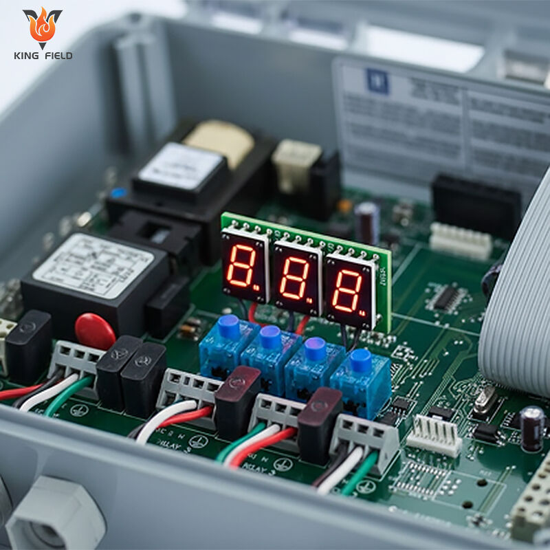
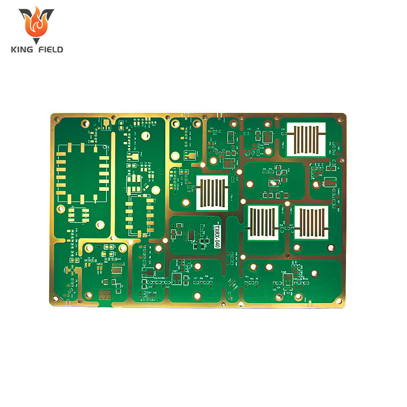
PCB prototyping is the process of creating a small batch of printed circuit boards that are fabricated, assembled, and tested to validate a design before commencing mass production. This vital step allows for hands-on verification and early identification of design flaws, manufacturing issues, and component problems.
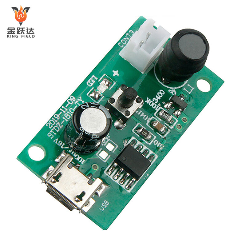
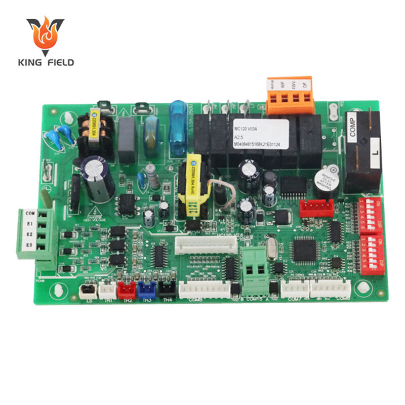
At its core, a PCB prototype is a physical realization of your PCB design—manufactured to the intended specifications but in limited quantity. The prototype serves as a working sample to:
Prototyping involves different levels depending on purpose and complexity:
|
Prototype Type |
Description |
Use Case |
|
Visual Model |
Physical or shape prototype with minimal or no electronics |
Enclosure fit, component layout visualization |
|
Proof-of-Concept Prototype |
Demonstrates primary function without full features or optimization |
Early functional validation |
|
Working Prototype |
Functional PCB incorporating planned features, used to identify design weaknesses |
Engineering development and debugging |
|
Functional Prototype |
Near-final version, often uses cost-saving materials; used for full validation and testing |
Pre-production testing and qualification |
Most prototypes use cost-effective materials like single- or double-sided FR-4 and standard finishes (OSP, HASL), while advanced prototypes for high-frequency or rugged applications may require multilayer stack-ups, rigid-flex laminates, or specialty substrates such as Nelco or Arlon.
Prototyping facilities offer rapid-turn capabilities, supporting:
A consumer electronics company relied heavily on quick-turn PCB prototyping services to iteratively refine their game controller design. Using multiple working and functional prototype cycles with comprehensive testing, they reduced costly design respins by 70% and accelerated volume production by 4 months.
Summary: PCB prototyping is a crucial checkpoint to validate and perfect your design. It bridges the gap between concept and production by addressing functional, mechanical, and manufacturability challenges early in the product lifecycle.
The PCB prototyping process is a collaborative and iterative journey involving designers, engineers, and manufacturers. The goal is to verify that the design functions correctly and meets all manufacturing constraints before mass production. Each step plays an essential role in delivering a quality prototype PCB that reflects the intended final product.
From concept to a working prototype, the process involves careful planning, detailed design work, fabrication, assembly, rigorous testing, and multiple iterations if needed. The key phases include:
Requirements Planning Clearly define product specifications, application requirements, and performance goals. Early input helps guide design choices that balance function, cost, and manufacturability.
Generation of PCB Schematics Use Electronic Design Automation (EDA) tools like Eagle or Altium to create circuit diagrams. Accurate schematics reduce risk of errors early in the design.
Bill of Materials (BOM) Creation Compile detailed lists of components including manufacturers, part numbers, quantities, and alternates. Efficient BOMs simplify sourcing and improve assembly accuracy.
Generation of PCB Layout Translate schematics into a physical board layout considering placement, routing, trace widths, and component spacing. Perform Design for Manufacturability (DFM) checks to optimize for fabrication and assembly.
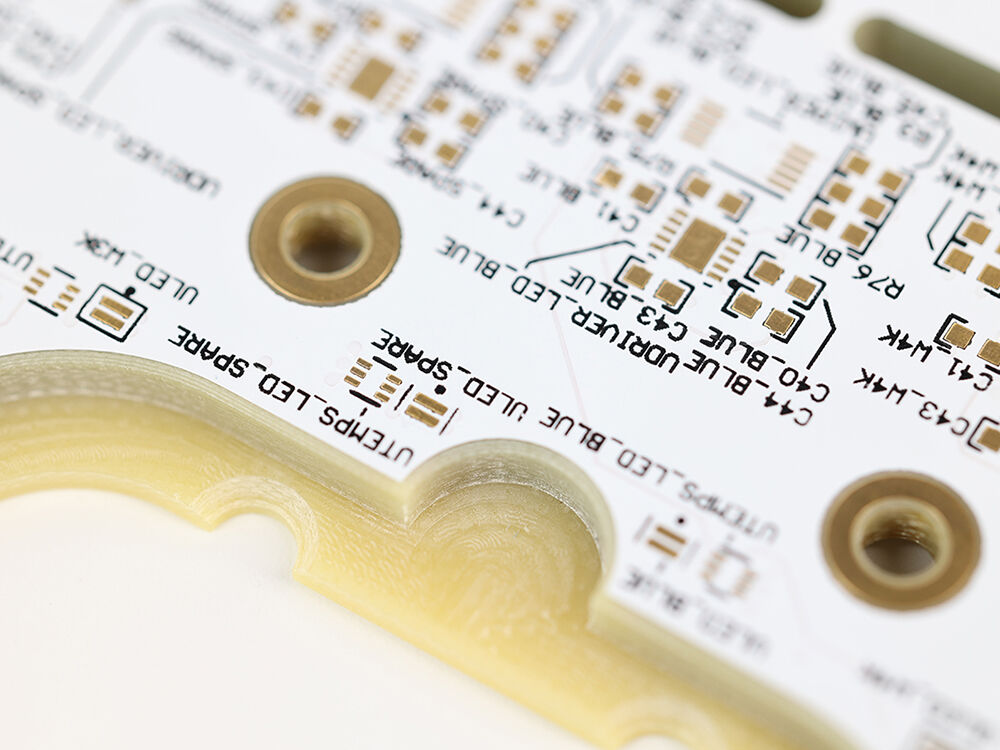
Design Rule Check (DRC) Run automated checks to ensure the design meets fabrication tolerances for trace spacing (often 0.005"–0.008"), hole sizes (minimum 0.010"–0.015"), and layer stack-up correctness.
Gerber File Generation Export fabrication files that precisely describe copper layers, solder mask, silkscreen, and drill data. These are the blueprints for PCB manufacturers.
PCB Fabrication Includes:
Bare PCB Testing Perform electrical tests to detect opens, shorts, and continuity problems in the unassembled board.
PCB Assembly Sequence includes:
Inspection and Testing
Design Iterations Based on test results, revise the design or processes and repeat prototyping until system requirements are met.
|
Step |
Typical Duration |
|
Design & DRC |
1–3 days |
|
Fabrication |
3–7 days |
|
Bare PCB Testing |
1 day |
|
Assembly |
1–3 days |
|
Inspection & Testing |
1–2 days |
|
Total (Prototype Cycle) |
~7–14 days (Rapid-Turn) |
A startup developing wearable fitness devices collaborated closely with their prototype PCB manufacturer. After the first prototype testing, minor DRC violations and thermal issues were identified. Rapid iterations enabled design corrections, resulting in improved manufacturability and a fully functional final prototype within three weeks. This careful phased process reduced expensive reworks later.
Embarking on the PCB prototyping phase brings a variety of critical advantages that directly impact cost, quality, and time-to-market for any electronic product. For startups and established manufacturers alike, these benefits are often the difference between a successful launch and costly delays or failures.
Building prototypes allows you to verify the manufacturing readiness of your board design. Issues such as incorrect trace widths, insufficient spacing, or thermal stress points that cause failures during production are identified early. This proactive approach leads to:
Prototyping provides a quality gate where electrical, mechanical, and functional properties are validated via:
Early testing reduces the risk of field failures, improving overall product reliability.
By uncovering design flaws and manufacturing challenges early, PCB prototyping cuts down the development cycle significantly. This enables:
Investing in PCB prototypes is far less expensive than scrapping large volumes of defective PCBs after mass production. Benefits include:
Physical prototypes serve as tangible tools to:
|
Benefit |
Description |
Impact |
|
Improved Yield |
Detect design and manufacturability issues early |
Higher first-pass fabrication success |
|
Enhanced Quality |
Thorough electrical and functional testing |
Increased reliability and compliance |
|
Accelerated Time-to-Market |
Faster iterations and reduced surprises |
Competitive product launch |
|
Cost Savings |
Minimized rework and recall costs |
Lower overall production expenses |
|
Stakeholder Communication |
Prototypes as visual and functional aids |
Better alignment and faster decision-making |
A startup designing innovative IoT sensors leveraged multilayer PCB prototyping combined with in-house DFM reviews and testing. Through multiple prototype runs, they identified a thermal dissipation issue undetected in simulations, corrected it, and optimized the PCB layout. This drastically improved product lifespan while saving approximately 20% in projected manufacturing costs.
In today’s fast-paced electronics landscape, PCB prototyping stands as an essential pillar for developing reliable, manufacturable, and high-quality printed circuit boards. By fabricating and testing prototype PCBs before committing to full-scale production, startups and manufacturers significantly reduce costly errors, accelerate time-to-market, and enhance overall product performance.
The prototyping process—from schematic development and design rule checks (DRC) to fabrication, assembly, and rigorous functional testing—provides invaluable insights that safeguard against design blind spots and production inefficiencies. Moreover, leveraging expert PCB prototyping services, especially those offering quick-turn capabilities and comprehensive assembly support, empowers teams to iterate swiftly and confidently transition from prototype to production.
Partnering with a trusted PCB manufacturer and assembly provider like Viasion Technology, which holds industry certifications such as ISO 9001:2015 and AS9100D, ensures access to advanced technologies and quality standards necessary to meet complex and evolving industry demands.
By embedding prototyping early in your product development, you foster innovation, optimize cost efficiency, and position your product for success in a competitive market.
 Hot News
2026-01-17
2026-01-16
2026-01-15
2026-01-14
2026-01-13
2026-01-12
2026-01-09
2026-01-08