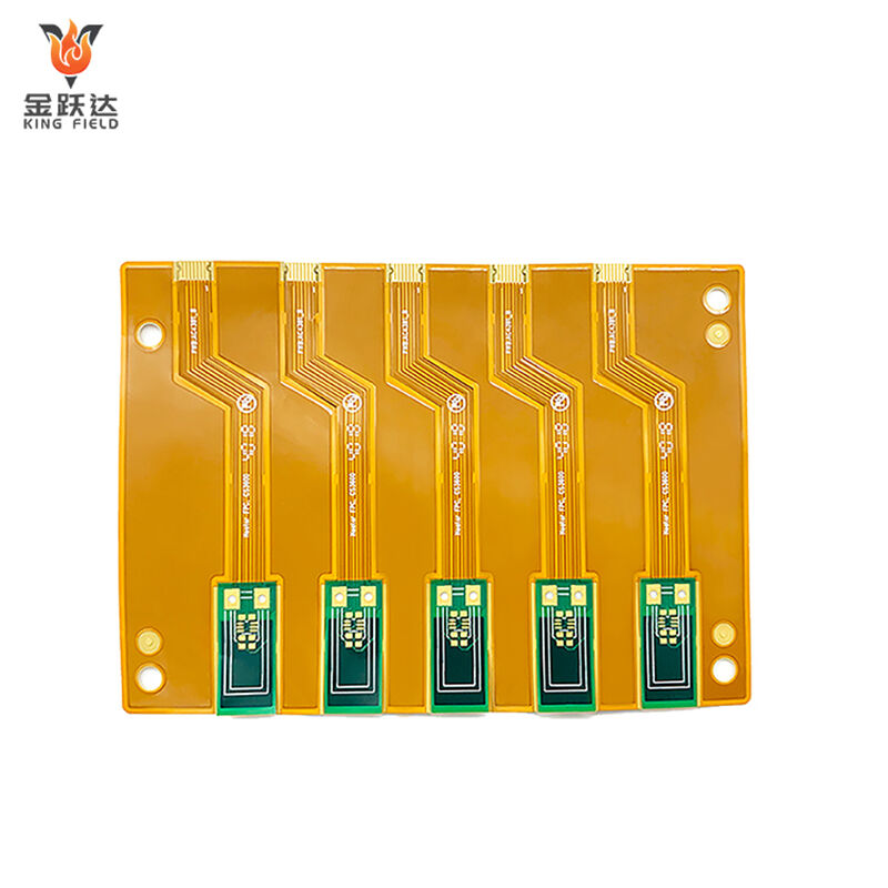
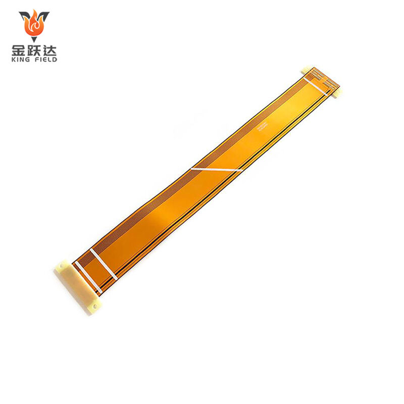
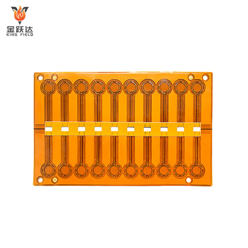
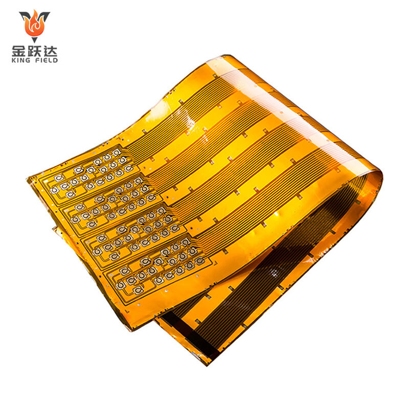
Flexible PCB
Custom Flexible PCB solutions for medical, industrial, automotive & consumer electronics. High precision, durable materials, fast prototyping & mass production. Adapt to tight spaces, complex designs—reliable performance, on-time delivery.
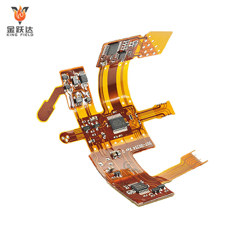
Description
What is a flexible PCB?
Future Development Trends of Flexible PCBs
With the rapid iteration of electronic technology and the surge in market demand for highly integrated, lightweight electronic products, flexible PCBs will occupy a core position in the future electronics industry due to their excellent adaptability, high durability, and design flexibility, becoming a key element driving industry innovation and development.
Advantages of flexible PCB
• High space utilization and flexible design: Flexible PCBs can be bent, folded, and rolled, greatly improving space utilization and allowing circuit designs to adapt to irregular shapes and curved surfaces, meeting the needs of thinner, more compact products and special applications.
• Superior durability and environmental adaptability: Utilizing high-performance substrates and copper-clad laminates, flexible PCBs possess excellent heat resistance, cold resistance, and chemical corrosion resistance, as well as good vibration and shock resistance. They maintain stable electrical performance in harsh environments, extending product lifespan.
• Excellent signal transmission and reliability: Fine-tuned circuit design reduces signal transmission interference and attenuation, improving signal quality and stability. Fewer connection points reduce the risk of failure, ensuring high circuit reliability.
• Efficient manufacturing and assembly advantages: Flexible PCBs support automated production, improving production efficiency. Their lightweight and flexible nature facilitates manual handling and adjustment, reducing assembly difficulty and cost.
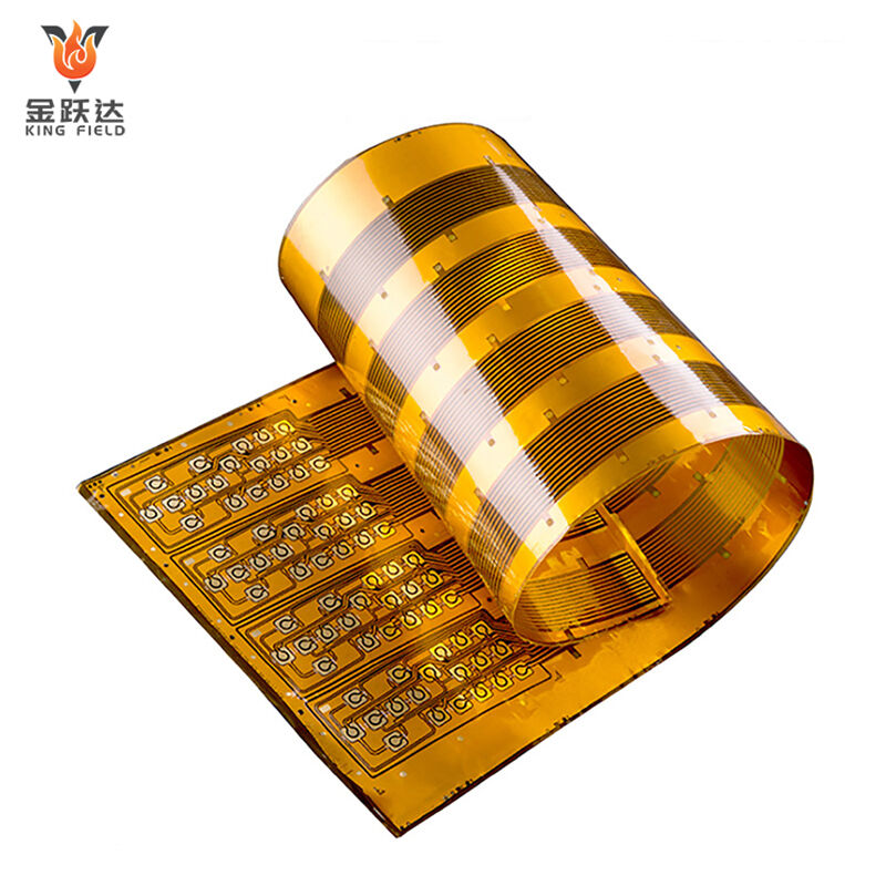
Materials for flexible PCBs
Performance comparison of polyimide (PI) and polyethylene terephthalate (PET)
| type | Polyester fiber (PET) | Polyimide Adhesive | Adhesive-free polyimide | |||
| Heat resistance | Temperature resistance: 100-200℃, short-term up to 230℃; prone to deformation at high temperatures | Long-term temperature resistance: 250-400℃, short-term resistance: over 500℃ | Long-term temperature resistance of 300-400℃, maintaining physical stability at high temperatures | |||
| Mechanical properties | High tensile strength, but brittle and easily broken | High tensile strength (170-400MPa), excellent bending resistance | High strength and fatigue resistance, tear resistance superior to PET | |||
| Chemical stability | Resistant to dilute acids and solvents, but generally has moderate hydrolysis resistance | Resistant to strong acids and alkalis, chemical corrosion, and radiation | Resistant to chemical solvents and hydrolysis, with good biocompatibility | |||
| Adhesive properties | Requires additional adhesives; peel strength is easily affected by temperature | Special adhesive requires surface treatment (sanding, cleaning); high bonding strength after curing | Achieves adhesive-free bonding through hot pressing or self-adhesive processes, reducing interface defects | |||
| Application scenarios | Suitable for medium- and low-temperature processes, consumer electronics | Suitable for high-temperature encapsulation (semiconductors, LEDs), aerospace, and medical devices | Suitable for high-end flexible circuits, high-temperature lamination, and biomedical devices | |||
| cost | Low temperature | High cost (complex special adhesives and processes) | Higher cost (adhesive-free processes reduce adhesive costs, but the material itself is expensive) | |||
Type
Flexible PCB type
| Single-layer flexible PCB | |
 |
• Structure: Composed of a single layer of copper foil, a substrate (such as PI or PET), and a cover film; the thinnest (0.05-0.2mm) with no interlayer interconnects. • Mechanical Properties: Optimal flexibility, capable of being bent repeatedly over 100,000 times, suitable for high-frequency dynamic deformation scenarios. • Electrical Properties: Low wiring density, supports only simple circuits; high-frequency signals are susceptible to interference, requiring jumpers to expand wiring space. • Cost: Lowest manufacturing cost; simple materials and processes, suitable for budget-sensitive applications. • Application Scenarios: Low-complexity connections, static or low-frequency bending devices. |
| Double-layer flexible PCB | |
 |
• Structure: Two layers of copper foil connected by vias, with a substrate and cover film sandwiched in one layer, thickness 0.15-0.3mm. • Mechanical Properties: Good flexibility, but bending radius needs to be controlled (≥0.1mm recommended) to avoid copper foil breakage at the vias. • Electrical Properties: Wiring density increased by more than 50%, supports medium-complexity circuits, and signal integrity can be optimized through shielding design. • Cost: Medium, requires via metallization process, manufacturing cost is 30%-50% higher than single-layer. • Application Scenarios: Dynamic devices, medium-density circuits requiring double-sided wiring. |
| Multilayer flexible PCB | ||
|
• Structure: Three or more layers of copper foil stacked together, interconnected vias/blind vias, thickness 0.2-0.6mm (increasing with the number of layers). • Mechanical Properties: Poor flexibility, requiring local reinforcement design to reduce bending stress, suitable for static or low-frequency deformation scenarios. • Electrical Properties: High wiring density, supports signal/power layered design, precise impedance control, suitable for high-speed signal transmission. • Technological Breakthrough: Employs microvia stacking technology (linewidth/spacing up to 20μm), graphene composite substrate improves heat dissipation (thermal conductivity 600W/m·K). • Cost: Highest, involving complex processes such as lamination, laser drilling, and electroplating, manufacturing cost is 2-3 times higher than single-layer. • Application Scenarios: High-density circuits, space-constrained scenarios requiring high performance. |
|
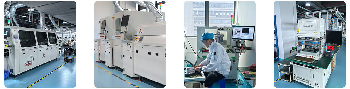
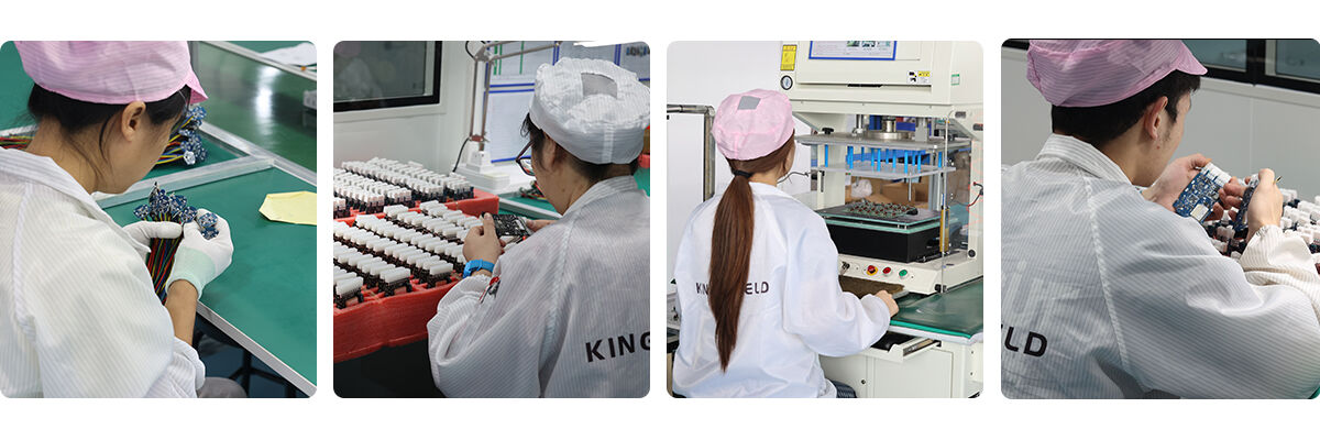
Kingfield offers one-stop manufacturing services for flexible, rigid-flexible, and rigid PCBs, using high-quality materials and advanced processes. It supports high-precision design and customization needs, providing rapid prototyping, free technical analysis, and reliable quality testing. With efficient delivery and excellent service, Kingfield has become the preferred partner for many companies.
Quality
Order PCB boards and PCB assembly services online.
We uphold the principle of price transparency, eliminating all hidden fees so you can understand your purchase clearly. All products are manufactured in our own factory, with strict control over the production process, providing you with reliable assurance of superior quality. We are a partner you can trust.
Manufacturing capacity
| PCB Manufacturing Capability | |||||
| ltem | Production capability | Min space for S/M to pad, to SMT | 0.075mm/0.1mm | Homogeneity of Plating Cu | z90% |
| Layer Count | 1~40 | Min space for legend to pad/ to SMT | 0.2mm/0.2mm | Accuracy of pattern to pattern | ±3mil(±0.075mm) |
| Production size(Min & Max) | 250mmx40mm/710mmx250mm | Surface treatment thickness for Ni/Au/Sn/OSP | 1~6um /0.05~0.76um /4~20um/ 1um | Accuracy of pattern to hole | ±4mil (±0.1mm ) |
| Copper thickness of lamination | 1/3 ~ 10z | Min size E- tested pad | 8 X 8mil | Min line width/space | 0.045 /0.045 |
| Product board thickness | 0.036~2.5mm | Min space between tested pads | 8mil | Etching tolerance | +20%0.02mm) |
| Auto-cutting accuracy | 0.1mm | Min dimention tolerance of outline (outside edge to circuit) | ±0.1mm | Cover layer alignment tolerance | ±6mil (±0.1 mm) |
| Drill size(Min/Max/hole sizetolerance) | 0.075mm/6.5mm/±0.025mm | Min dimention tolerance of outline | ±0.1mm | Excessive adhesive tolerancefor pressing C/L | 0.1mm |
| Min percent for CNC slot length and width | ≤0.5% | Min R corner radius of outline(inner filleted corner) | 0.2mm | Alignment tolerance forthermosetting S/M and UV S/M | ±0.3mm |
| maximum aspect Ratio(thickness/hole diameter) | 8:1 | Min space golden finger to outline | 0.075mm | Min S/M bridge | 0.1mm |
Frequently Asked Questions
Q1: What are the suitable applications for flexible PCBs?
KING FIELD: Suitable for applications requiring bending, lightweighting, or space constraints, such as wearable devices, foldable phones, automotive electronics, and medical endoscopes.
Q2: What are the commonly used substrates for flexible PCBs? How to choose?
KING FIELD: Commonly used substrates are polyimide and polyester. Choose PI for high-temperature or harsh environments, and PET for low-temperature applications such as consumer electronics.
Q3: What precautions should be taken when bending flexible PCBs?
KING FIELD: The minimum bending radius should be ≥ 5-10 times the board thickness; the traces in the bending area should be perpendicular to the bending axis, avoiding vias; reinforced areas should be reinforced to prevent deformation.
Q4: Are flexible PCB soldering problems prone to occur? How to solve them?
KING FIELD: The flexibility of the material can easily lead to poor soldering or solder joint detachment. Solution: Low-temperature soldering (≤245℃), use of high-precision pick-and-place machines, and AOI/X-Ray detection of hidden defects.
Q5: How much more expensive are flexible PCBs than rigid PCBs? Are they worth choosing?
KING FIELD: The cost is usually 30%-50% higher, but they save space, reduce weight, and improve reliability. Flexible PCBs are a better choice if the equipment requires frequent bending or space is limited.

