Rogers PCB
High-performance Rogers PCBs for RF/telecom/automotive/industrial high-frequency applications. Premium Rogers materials
(RO4003C/RO5880), ultra-low loss & precise impedance control—optimized for GHz signal integrity.
✅ Low-loss Rogers substrates
✅ Precise impedance control (±5%)
✅ RF/microwave/high-speed data focus
Description
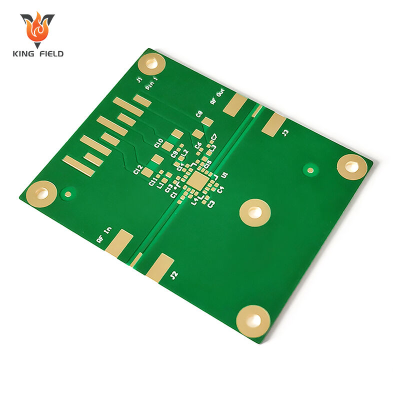
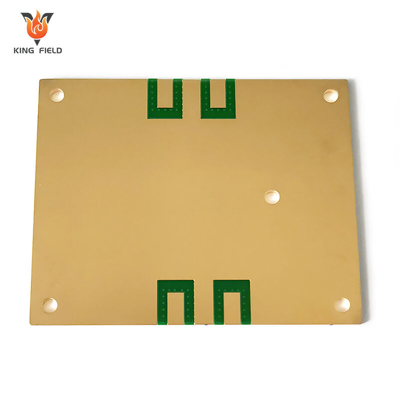
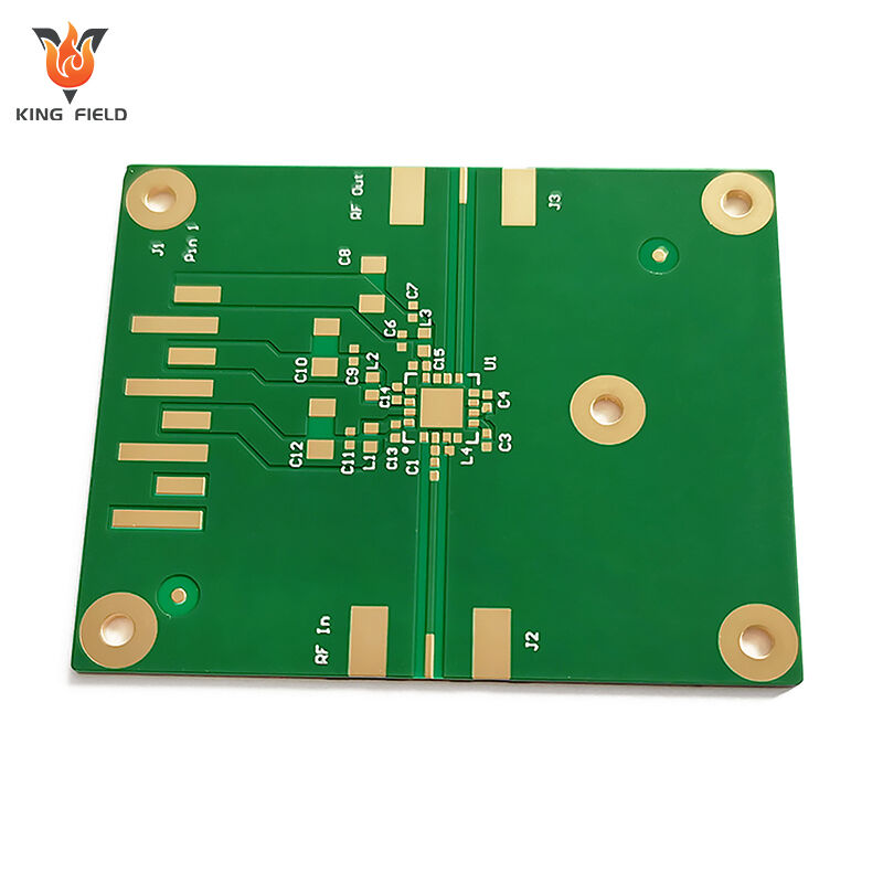
What is Rogers PCB?
Rogers PCB refers to a high-performance printed circuit board manufactured using specialized laminate materials produced by Rogers Corporation, an American advanced materials and technology enterprise. Unlike conventional FR-4 PCBs which are made from epoxy resin and glass fiber, it mainly adopts materials such as polytetrafluoroethylene (PTFE), ceramic-filled composites, or hydrocarbon blends. It is especially suitable for high-frequency and high-speed electronic scenarios and is known as the benchmark in related fields. The following is a detailed introduction:
Core Material Series
| Material Series | Key Characteristics | Typical Application Scenarios | |||
| RO4000 Series | It has cost-effectiveness, good processability, stable dielectric constant, and low dielectric loss. For example, RO4350B has a stable dielectric constant around 3.48 and excellent thermal stability. | 5G communication modules, high-frequency antennas, and radio frequency circuits. | |||
| RT/duroid Series | It is based on fluoroplastics, featuring extremely low dielectric loss and outstanding high-frequency performance. RT5880 is a representative product. | Microwave circuits, precision radar systems, and high-end test instruments. | |||
| RO3000 Series | It is a reinforced fluoroplastic material with good dimensional stability and moisture resistance. | Commercial microwave equipment and medium-to-high-end RF communication devices. | |||
| TMM Series | As a hydrocarbon ceramic material, it combines the advantages of ceramics and hydrocarbons, with high thermal conductivity and stable electrical properties. | High-power RF components and high-temperature operating electronic equipment. | |||
Advantages and Applications
Outstanding Performance Advantages
Low Signal Loss:
Its materials have a low dissipation factor. When signals are transmitted at frequencies above 2GHz, the loss is far lower than that of traditional FR-4 PCBs, which effectively ensures signal integrity.
Stable Dielectric Properties:
The dielectric constant remains stable within a wide range of temperature and frequency. This allows engineers to accurately design circuits such as impedance matching and transmission lines.
Strong Environmental Adaptability:
Many materials in its series have low water absorption, enabling stable operation in high-humidity environments. Meanwhile, they have high glass transition temperatures (generally above 280°C) and excellent thermal stability, which can tolerate extreme temperature changes.
Main Application Fields
Telecommunications:
It is a core material for 5G base station RF modules, millimeter-wave antennas, and satellite communication equipment, which meets the demand for low-loss and high-speed signal transmission in communication systems.
Aerospace and Defense:
It is applied to radar systems, missile guidance modules, and space-borne electronic equipment. Its low outgassing performance and resistance to harsh environments can adapt to the complex conditions of space and battlefield.
Automotive Electronics:
It is used in automotive radar, vehicle-mounted 5G communication modules, and new energy vehicle power control systems, which can withstand the high-temperature and high-vibration working environment in vehicles.
Test and Measurement Instruments:
It is used in high-frequency signal generators, vector network analyzers, and other precision instruments, which guarantees the accuracy and stability of instrument measurements.
Precautions
Due to the significant differences in substrate characteristics between rogers pcb board and traditional FR-4 PCBS, the manufacturing process requires targeted control of process details. The core points to note are as follows:
Substrate treatment and storage
· Storage conditions:
Rogers base materials (especially PTFE base materials) are prone to moisture absorption and should be stored in a constant temperature and humidity environment. If not used promptly after opening, they should be vacuum-packed and sealed to prevent moisture absorption, which may cause bubbles and delamination during welding.
· Base material cutting:
Use dedicated hard alloy tools for cutting to prevent edge cracking of the base material. After cutting, the edge debris should be cleaned up to prevent scratching the board surface during subsequent processing.
· Surface cleaning:
Do not use strong corrosive cleaning agents on the substrate surface. Isopropyl alcohol is preferred for wiping to remove oil stains or dust, avoiding contamination that may affect the bonding strength of the copper layer.
Drilling and forming process
· Drilling parameters:
PTFE-based Rogers material has high hardness and poor thermal conductivity. When drilling, diamond-coated drill bits should be selected. Reduce the rotational speed, increase the feed rate, and at the same time enhance cooling to prevent drill bit wear or base material ablation. For aluminum nitride-filled substrates, it is necessary to avoid the formation of micro-cracks during drilling. A step-by-step drilling method can be adopted.
· Hole wall treatment:
After drilling, plasma cleaning or chemical etching is required to remove the residual substrate debris on the hole wall, ensuring the adhesion of metallization on the hole wall.
Avoid excessive etching that may cause rough hole walls and affect the uniformity of the coating.
· Shape forming:
CNC precision engraving or laser cutting is adopted to avoid blanking. After cutting, the edges need to be ground to remove burrs.
Metallization and electroplating
· Copper plating pretreatment:
The surface of Rogers substrate is highly inert (especially PTFE), so special roughening processes need to be adopted to increase the surface roughness of the substrate and enhance the adhesion of the copper plating layer. Avoid excessive roughening that may cause damage to the substrate surface.
· Electroplating parameters:
When electroplating copper, the current density needs to be reduced (15% lower than FR-4), the electroplating time should be prolonged, and the coating should be uniform. For thick copper designs (≥2oz), segmented electroplating should be adopted to prevent uneven coating thickness or pinholes.
· Coating inspection:
Focus on checking the coverage and adhesion of the coating on the hole wall. The adhesion of the coating on the hole wall of PTFE-based Rogers PCBS should be ≥1.5N/mm to prevent coating peeling during subsequent use.
Etching and circuit fabrication
· Etching solution selection:
Use acidic etching solutions (such as copper chloride system) to avoid alkaline etching solutions from corroding Rogers substrates (some ceramic-filled substrates have poor alkali resistance); During the etching process, the temperature (25 to 30℃) and etching speed must be strictly controlled to prevent excessive side etching, which could lead to a decrease in the accuracy of the circuit.
· Line compensation:
Preset the etching compensation amount according to the base material type to ensure that the final line width meets the design requirements; For fine lines (line width < 0.1mm), high-precision exposure equipment should be used to avoid broken lines or short circuits.
Solder mask and surface treatment
· Solder mask ink compatibility:
Select high-temperature resistant solder mask ink (Tg > 150℃) that is compatible with Rogers substrates to prevent the ink from peeling off due to poor adhesion to the substrate. When printing solder mask, the pressure of the scraper should be reduced to prevent ink from seeping into the gap of the circuit.
· Curing process:
The curing temperature for solder mask should be increased step by step (from 80℃ to 150℃ gradually) to avoid deformation of the substrate caused by sudden temperature rise. The curing time is 10% to 20% longer than that of FR-4 to ensure complete curing of the ink.
· Surface treatment selection:
Prioritize gold plating (ENIG) or tin plating, and avoid hot air leveling (HASL) - high-temperature hot air can cause the Rogers substrate to warp, and PTFE base materials have limited heat resistance.
Lamination process
· Lamination parameters:
Set the lamination temperature, pressure and time according to the type of substrate to avoid substrate decomposition due to excessively high temperature or delamination due to uneven pressure.
· Glue removal treatment:
Before lamination, the precured sheet (PP) needs to be pre-baked at 100℃ for 30 minutes to remove volatile substances and prevent the formation of bubbles during lamination. The combination of Rogers substrate and PP needs to match the coefficient of thermal expansion to reduce warpage after lamination.
· Flatness control:
After the multi-layer Rogers PCB is laminated, it needs to be cold-pressed and set. The cooling rate should be controlled at 5℃/min to avoid excessive temperature difference causing warping of the board surface (the warping degree should be ≤0.3%).
Testing and quality control
· Electrical performance testing:
Focus on inspecting the line impedance, insertion loss, and standing wave ratio. Use a network analyzer to conduct full-range testing within the designed frequency band to ensure that the high-frequency performance meets the standards.
· Reliability testing:
Conduct thermal cycling tests and damp heat tests to verify the bonding stability between the substrate and the copper layer, as well as the solder mask layer, to prevent failure caused by environmental aging.
· Appearance inspection:
Check the board surface for cracks, delamination, bubbles, smooth edges of the circuits, and burrs on the hole walls to ensure there are no obvious appearance defects.
Rigid RPCB Manufacturing Capability
| Item | RPCB | HDI | |||
| minimum linewidth/linespacing | 3MIL/3MIL(0.075mm) | 2MIL/2MIL(0.05MM) | |||
| minimum hole diameter | 6MIL(0.15MM) | 6MIL(0.15MM) | |||
| minimum solder resist opening (single-side) | 1.5MIL(0.0375MM) | 1.2MIL(0.03MM) | |||
| minimum solder resist bridge | 3MIL(0.075MM) | 2.2MIL(0.055MM) | |||
| maximum aspect Ratio (thickness/hole diameter) | 0.417361111 | 0.334027778 | |||
| impedance control accuracy | +/-8% | +/-8% | |||
| finished thickness | 0.3-3.2MM | 0.2-3.2MM | |||
| maximum board size | 630MM*620MM | 620MM*544MM | |||
| maximum finished copper thickness | 6OZ(210UM) | 2OZ(70UM) | |||
| minimum board thickness | 6MIL(0.15MM) | 3MIL(0.076MM) | |||
| maximum layer | 14 layer | 12 layer | |||
| Surface treatment | HASL-LF、OSP 、Immersion Gold、 Immersion Tin 、Immersion Ag | Immersion Gold、OSP、selectiveimmersion gold、 | |||
| carbon print | |||||
| Min/max laser hole size | / | 3MIL / 9.8MIL | |||
| laser hole size tolerance | / | 0.1 |