Quick Links
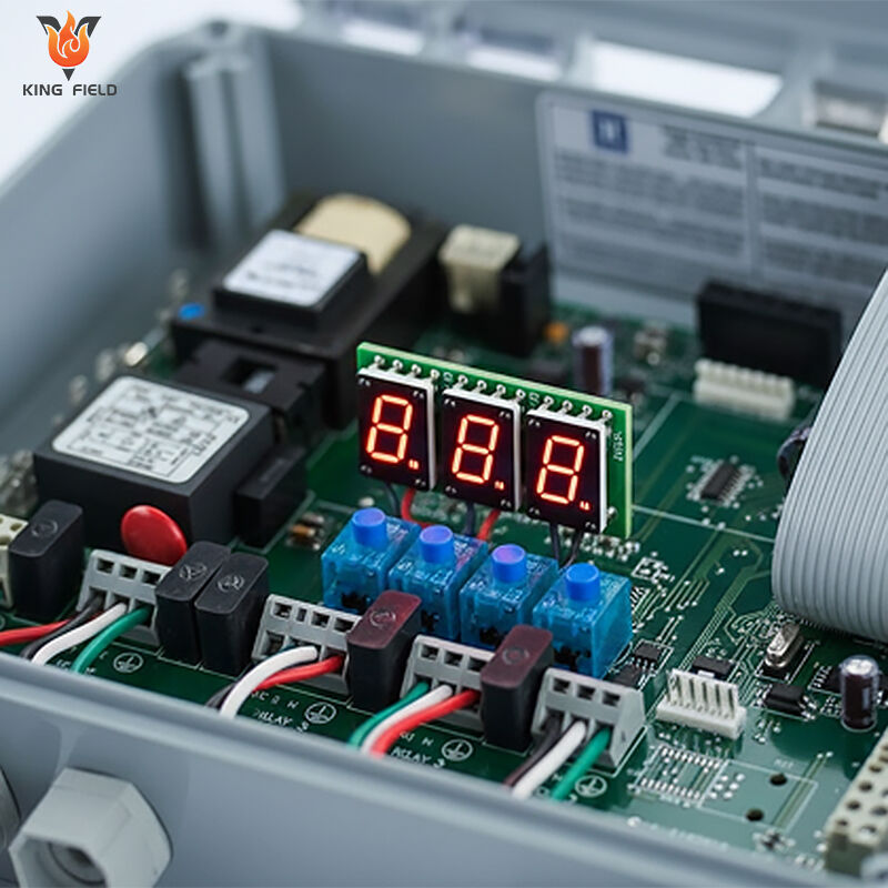
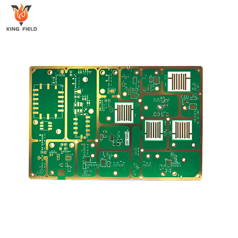
High-Density Interconnect PCBs, or HDI PCBs, represent one of the most advanced forms of circuit board technology, enabling today’s cutting-edge automotive electronics. Unlike conventional printed circuit boards, HDI PCBs incorporate microvias, ultra-fine trace and space, and complex via structures such as blind vias and buried vias to dramatically increase component density and routing flexibility.
At its core, HDI technology is defined by its higher wiring density—more conductors per unit area—and the ability to support extremely fine trace widths and minimal spacing between traces. These characteristics allow designers using HDI PCBs to:
|
Feature |
Description |
|
Microvia Technology |
Small-diameter vias (<150 μm) drilled using precise laser drilling. |
|
Blind and Buried Vias |
Allow routing connections between selected layers, eliminating unnecessary drilling. |
|
Sequential Lamination |
Enables complex stackups with multiple lamination cycles and via structures. |
|
Fine Line Capability |
Trace width and space as tight as 1-mil, supporting dense routing. |
|
Via Structures |
Includes through-hole vias, stacked microvias, staggered microvias, via-in-pad. |
|
Advanced Plating |
High-reliability plating for microvia filling and copper deposition. |
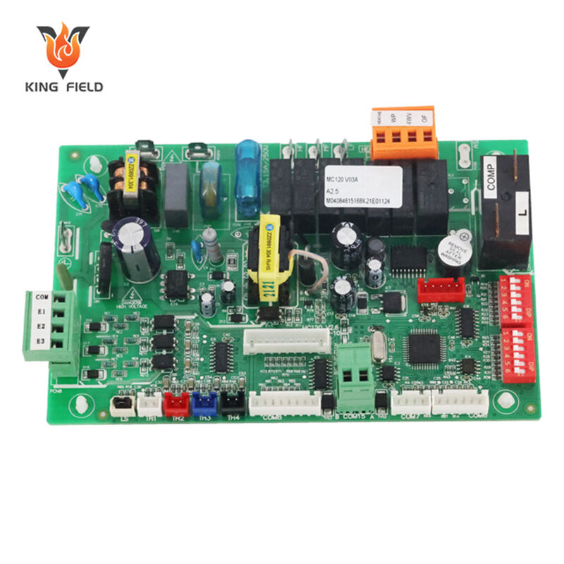
The push towards miniaturization and increased functionality in vehicles—such as infotainment modules, ADAS, and battery management—has driven the adoption of HDI in automotive applications. The compact, advanced stackup enabled by HDI technology not only reduces the footprint and weight of automotive electronics but also enhances reliability by enabling shorter, controlled-impedance signal paths that are crucial for high-speed data transmission.
|
Via Type |
Description |
Typical Use-Case |
|
Through-Hole |
Drilled from surface to surface; all layers |
Power/ground, legacy components |
|
Blind Via |
Connects outer layer to inner layer(s) but not through entire board |
BGA breakout, tight routing |
|
Buried Via |
Connects only inner layers; not visible on outside |
Dense, multi-layer interconnect |
|
Microvia |
Laser-drilled, very small diameter (<150 μm), typically for HDI stackups |
Fine-pitch devices, signal integrity |
|
Stacked Microvia |
Microvias stacked directly atop one another across multiple layers |
3+ lamination cycles, densest boards |
|
Staggered Microvia |
Microvias offset from each other in subsequent layers |
Improved reliability, manufacturability |
Routing Density vs. Layer Count: Optimize signal breakout and return path using tools like stackup designers; more layers often allow cleaner, more robust routing with less crosstalk.
Not all vehicle PCBs are HDI—but HDI is essential for complex, compact designs. Automotive needs various PCB types, with modern vehicles using:
|
HDI PCB Type |
Key Features & Technologies |
Common Automotive Use-Cases |
|
Through-Hole HDI |
Combines through-hole vias and microvias |
Power distribution, sensors |
|
Sequential Build-Up (SBU) |
Layer-by-layer sequential lamination, microvias, fine line |
Infotainment, ADAS central processing, ECUs |
|
Rigid-Flex HDI |
Combines rigid layers with flexible circuits, often with microvias |
Head-up display modules, foldable displays, sensors |
|
Any-Layer HDI |
Microvias between all adjacent layers (“HDI any-layer”) |
Mission-critical ECUs, radars, automotive cameras |
|
Build-Up (Coreless) |
Ultra-thin stackups, microvias, special press-out thickness |
Miniature modules, key fobs, compact wireless devices |
|
Cavity-Based HDI |
Board cavities for embedding chips, custom stackups |
Camera modules, radar/ultrasonic sensors, LiDAR units |
When specifying HDI PCBs for automotive applications, several key requirements should be defined up front. These parameters will directly impact stackup selection, via structure, manufacturability, and PCB cost:
|
Parameter |
Typical Value / Range |
Notes |
|
PCB Layers |
6–12 |
Driven by design complexity |
|
Min. Trace/Space |
2-mil (50 µm) / 1-mil (25 µm possible) |
SEMI-ADDITIVE for ultra-fine lines |
|
Smallest BGA Pitch |
0.4 mm or less |
Demands microvias, via-in-pad |
|
Microvia Aspect Ratio |
≤ 0.75:1 |
Promotes reliable plating |
|
Finished Board Thickness |
1.0–1.6 mm |
Customize as per application |
|
Via Structure |
Stack-up-specific (see below) |
Stacked, staggered, through-hole |
|
Material Tg |
>170°C (high-Tg FR-4, polyimide) |
For thermal reliability |
|
Controlled Impedance |
Yes, typically ±10% |
Essential for high-speed signals |
|
Compliance |
RoHS, WEEE, Automotive (IATF) |
Must be communicated |
Selecting an automotive HDI PCB manufacturer is not just about technology—it’s about trust. The stakes in automotive electronics are high: failures can have safety implications, lead to costly recalls, and damage brand reputations. That’s why leading manufacturers invest heavily in quality certifications, advanced process controls, and continuous improvement systems for every step of the HDI PCB fabrication process, from microvia plating to sequential lamination and final assembly.
Choosing a partner with the right industry certifications is non-negotiable in the automotive sector. These certificates guarantee adherence to stringent quality management, traceability, and process control standards. Here’s what to look for:
|
Certification |
Description & Relevance |
Automotive Importance |
|
IATF 16949 |
Automotive sector quality management (based on ISO9001) |
Mandatory for car OEMs |
|
ISO 9001:2015 |
Top-level global quality standard |
Assures process discipline |
|
AS9100D |
Aerospace/defense quality |
Additional rigor (optional) |
|
UL Certification |
Safety and flammability compliance |
Needed for legal sale |
|
RoHS & WEEE |
Environmental, hazardous substance restrictions |
Regulatory EU/Asia req’t |
|
ISO 13485 |
Medical device focus (useful for auto medical subsystems) |
Niche, increases trust |
Automotive HDI PCBs must meet rigorous standards for traceability, repeatability, and defect prevention. The best manufacturers adopt a layered, end-to-end approach:
All base materials (FR-4, high-Tg, halogen-free, copper foil) are checked for conformance and traceability before production begins.
Automated Optical Inspection (AOI): Every layer is scanned with AOI to detect shorts, opens, and trace issues.
Drill Registration Checks: Microvia and laser drilling accuracy verified to ±1 mil to prevent misalignment, especially critical in staggered and stacked microvia structures.
Plating Thickness Monitoring: Ensures uniform copper plating in microvias for reliable conductivity and durability.
Statistical Process Control: Key steps (lamination, drilling, plating cycles) are monitored for variation; out-of-spec runs are stopped and investigated immediately.
HDI PCB supply impacts the entire automotive manufacturing chain. A top HDI PCB manufacturer provides:
To ensure PCB manufacturability and robust operation throughout the vehicle’s lifecycle, these standards must be built into the manufacturer’s workflow:
Materials in high-density interconnect PCBs must balance three main needs: electrical performance, mechanical robustness, and cost. The choices you make here echo through every step of manufacturing—impacting stackup, microvia reliability, plating consistency, and ultimately, total PCB cost.
|
Material Type |
Attributes |
Automotive Use Case |
|
High-Tg FR-4 |
Cost-effective, Tg >170 °C |
ECUs, infotainment, sensors |
|
Polyimide |
High-temp, flexible, robust |
Rigid-flex, engine bay, LED modules |
|
Halogen-Free Epoxy |
RoHS/WEEE, good CTE match |
Instrument clusters, interior lighting |
|
Ceramic-fill Hybrid |
Best thermal conductivity |
Power control, inverters, battery boards |
Reliability is non-negotiable in the automotive sector. Top-tier HDI PCB suppliers offer a battery of tests—both during material selection and after board fabrication—to ensure robust performance over the lifetime of the vehicle.
Temperature Cycling
Simulates the start/stop and daily operating swings (-40°C to +125°C or more).
Evaluates crack/void formation in microvias, blind vias, and plating.
Thermal Shock
Rapid heating and cooling to test for CTE-mismatch failures—critical for stacked microvias.
Moisture and Insulation Resistance
Essential for boards exposed to condensation or humidity, such as door modules.
Vibration/Mechanical Shock
Recreates the stresses of road travel and engine vibration.
Verifies adhesion of via fill material, solder joints, and overall stackup resilience.
Solderability & Reflow Cycles
Evaluates the robustness of conductive and non-conductive hole fill (NCF), especially with repeated assembly line reflow.
Microsection (Cross-section) Analysis
Inspects internal layers, copper plating thickness, and examines for via voids or delamination in sequential lamination HDI builds.
|
Test Name |
Method |
Typical Acceptance Criteria |
|
Temp Cycling |
−40 °C to +125 °C, 1000 cycles |
<5% electrical parameter shift |
|
Thermal Shock |
−55 °C to +125 °C, 300 cycles |
No visible cracks, no open circuits |
|
Solderability |
3–5 reflow cycles, IPC/JEDEC J-STD |
No pad lifting, no via fill extrusion |
|
Cross-section |
Metallographic analysis |
No voids >5%, fill >95% in microvias |
|
Vibration |
Varies, ISO/IEC standards |
Solder and stackup integrity, no cracks |
Microvias are tiny, laser-drilled holes (typically <150 µm diameter) that electrically connect densely routed layers without the drawbacks of large through-holes. Their small size is essential in supporting tight pitch components like 0.4 mm BGAs and maximizing routing density.
|
Parameter |
Typical Value |
Relevance to Automotive PCB |
|
Drill diameter |
≤ 0.15 mm (150 µm) |
Enables thin pad/via-on-pad for 0.4 mm BGA |
|
Aspect ratio |
< 0.75:1 |
Improves plating integrity, reliability |
|
Pad size |
≥ 0.25 mm |
Ensures registration and robust soldering |
|
Via Type |
Drilling Method |
Typical Use |
Pros |
Cons |
|
Through-hole via |
Mechanical |
Power/ground, older tech |
Simple, lower cost |
Consumes more real estate |
|
Blind via |
Laser |
BGA breakout, compact modules |
Frees up surface |
More complex fabrication |
|
Buried via |
Laser/Mechanical |
Deep stack routing |
No surface space lost |
Harder to inspect |
|
Microvia |
Laser |
High-density layers |
High density, reliable |
Limits on aspect ratio |
|
Staggered microvia |
Laser |
Reliability, dense stackups |
Less stress, high yield |
Complex registration |
|
Stacked microvia |
Laser |
Ultra-high pin-count BGAs |
Maximizes density |
More lamination/plating steps |
|
Stackup Type |
Description |
Automotive Usage |
|
1-N-1 |
One build-up layer per side |
Entry-level HDI, sensors |
|
2-N-2 |
Two build-up layers per side |
BGA, infotainment |
|
3-N-3 |
Three build-up layers per side, sometimes coreless |
Radar, computing, telematics |
|
Hybrid stackup |
Combination of different materials/stackups |
Power-plus-signal, ruggedized ECUs |
Choosing the best automotive HDI PCB manufacturer means looking far beyond just technology and capability—you must also weigh the factors that drive total PCB cost, delivery reliability, and the quality of ongoing support you will receive. In automotive projects, a misstep in any of these areas can cause costly delays, blown budgets, and downstream quality headaches.
The cost structure of HDI PCB manufacturing is more complex than traditional PCBs due to the technical sophistication of processes such as laser drilling, sequential lamination, and advanced via structure fabrication. Here’s a breakdown of the primary cost drivers:
|
Stackup & Feature |
Estimated Cost Impact (%) |
|
Simple 1-N-1 stackup |
Baseline (no increase) |
|
2-N-2 stackup |
+25–30% |
|
3-N-3 with stacked microvias |
+40–60% |
|
Fine line (1-mil SAP) |
+20–35% |
|
Conductive via-in-pad |
+15–25% |
|
High-Tg HAL-free material |
+10–15% |
The process of choosing the right automotive HDI PCB manufacturer is critical for ensuring both short-term project success and long-term vehicle reliability. With so many vendors touting advanced HDI capabilities, it’s vital to look past marketing claims and evaluate potential partners using a rigorous, multidimensional checklist.
A supplier’s track record matters—especially in automotive, where reliability is non-negotiable.
|
Feature |
Supplier A (Automotive Specialist) |
Supplier B (General PCB Shop) |
|
Years in Business |
25 |
7 |
|
IATF 16949 Certification |
Yes |
No |
|
Stackup/Drill Capabilities |
3-N-3, staggered microvias, SAP |
1-N-1, through-hole only |
|
Automotive Clients |
8 Tier 1s, 2 OEMs |
Few, mainly consumer |
|
Proto Turn Time |
3 days |
10 days |
|
Engineering Support |
Dedicated DFM/Stackup team |
Email-only, generic advice |
|
Cost Transparency |
Full itemized, clear NRE/DFM |
Lump sum, unclear cost drivers |
Check if suppliers stay current or push boundaries:
A central element in any high-quality automotive HDI PCB is the stackup—the layered structure of the board which determines signal performance, physical strength, thermal robustness, and manufacturability. The right HDI stackup also ensures optimal routing density for tight-pitch components while managing cost and process risk. Automotive applications often require more complex stackups than commercial devices due to demands for ruggedness, tight BGA breakout, controlled impedance, and long-term reliability.
|
Stackup Type |
Typical Layers |
Key Features |
Automotive Example |
|
1-N-1 |
4–6 |
Entry HDI, single microvia |
Sensors, non-safety ECUs |
|
2-N-2 |
8–10 |
Stacked microvias, buried via |
High-pin BGAs, infotainment, ADAS |
|
3-N-3 |
>10 |
Coreless, hybrid, SAP process |
Radar, telematics, compute ECUs |
|
Stackup |
Min. Trace/Space |
BGA Pitch Supported |
Routable BGA I/O (per 1000 pins) |
Lam Cycles |
|
1-N-1 |
4/4 mil |
0.65 mm |
600–700 |
2–3 |
|
2-N-2 |
2/2 mil |
0.4 mm |
850–900 |
4–5 |
|
3-N-3+ |
1/1–2/2 mil |
<0.4 mm |
>950 |
6+ |
Best Practice: Involve your HDI PCB supplier’s stackup designer and DFM engineers at project outset, especially when high complexity, fine-line routing, or severe environmental specs are required.
As vehicles accelerate toward higher levels of automation, electrification, and digital connectivity, the demands on automotive HDI PCBs are rapidly evolving. Tomorrow’s vehicles will require even more advanced high-density interconnect (HDI) solutions—pushing the boundaries of stackup complexity, miniaturization, signal integrity, and manufacturability.
|
Trend |
Description |
Automotive Benefit |
|
Coreless stackups |
No rigid internal core; lighter, more flexible |
Camera modules, EV battery sensors |
|
Ultra-fine SAP lines |
1-mil routing, increased density |
Smaller modules, smarter dashboards |
|
Embedded passives |
RC components built into layers |
EMI, signal integrity improvement |
|
Cavity HDI |
Precision board cutout for stacked dies or MEMS |
Thinner radars, better packaging |
 Hot News
2026-01-17
2026-01-16
2026-01-15
2026-01-14
2026-01-13
2026-01-12
2026-01-09
2026-01-08