Quick Links
Electronics are the backbone of our modern world, powering everything from simple wearables to advanced aerospace equipment. At the core of every electronic device lies the PCB (Printed Circuit Board) and, by extension, the PCBA (Printed Circuit Board Assembly).
This guide will help you master:
The definitions and core functions of PCBs and PCBAs.
The complete PCB manufacturing process and PCB assembly process.
Key PCB types and how they are used in consumer electronics, medical devices, automotive controls, and more.
Decision factors for choosing bare boards vs. assembled solutions.
Parameters that shape cost, performance, reliability, and lead time.
FR-4 (most common): Offers a balance of strength, thermal stability, and electrical insulation.
High-frequency laminates: Such as Rogers, ideal for RF/microwave and high-speed/high-frequency circuits due to lower dielectric loss.
Polyimide: Used for flexible and rigid-flex PCBs, excellent for dynamic bending and heat resistance.
Aluminum-core: For high-power LED and automotive applications requiring efficient thermal management.How to select a partner for PCB manufacturing, PCB assembly services, and rapid prototyping.
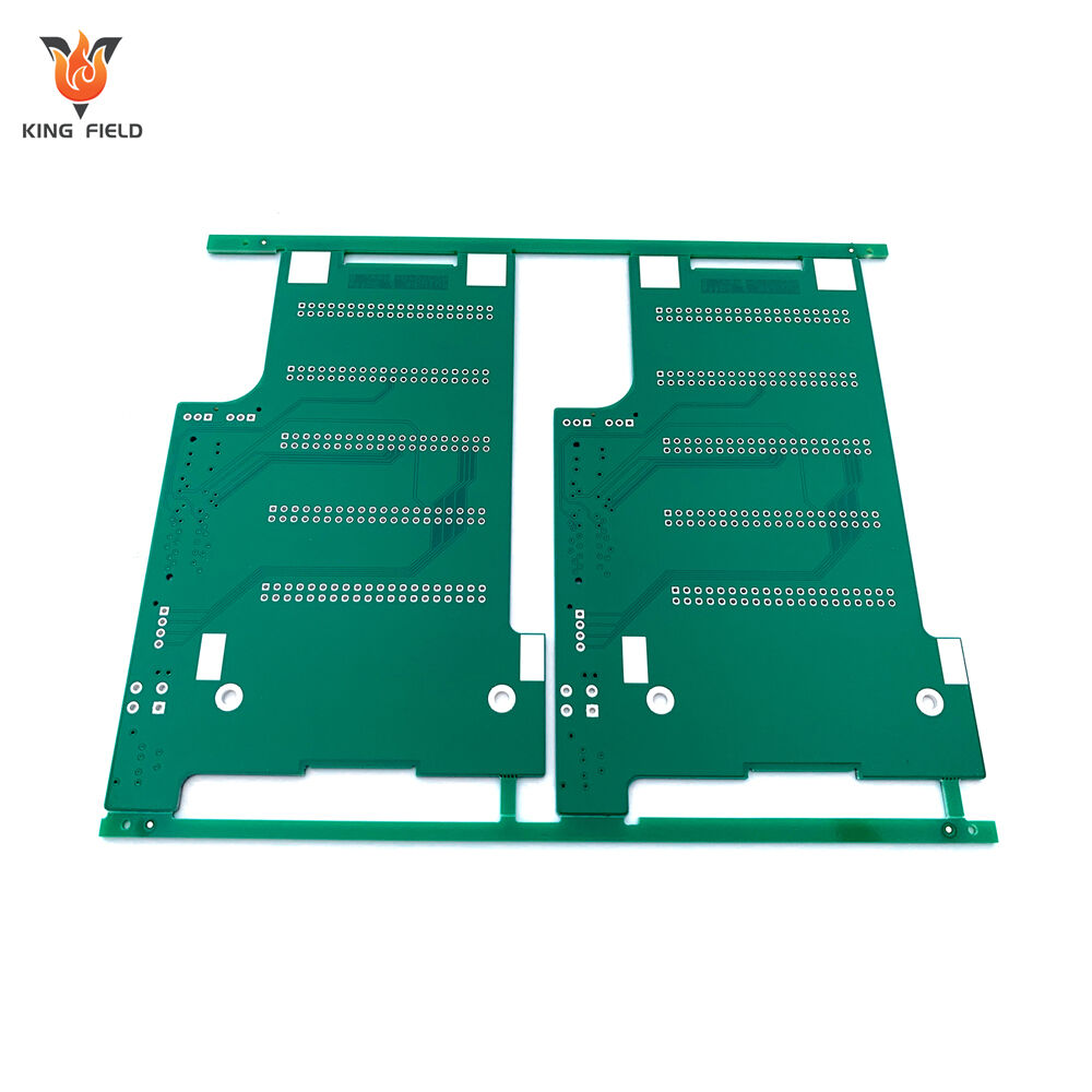
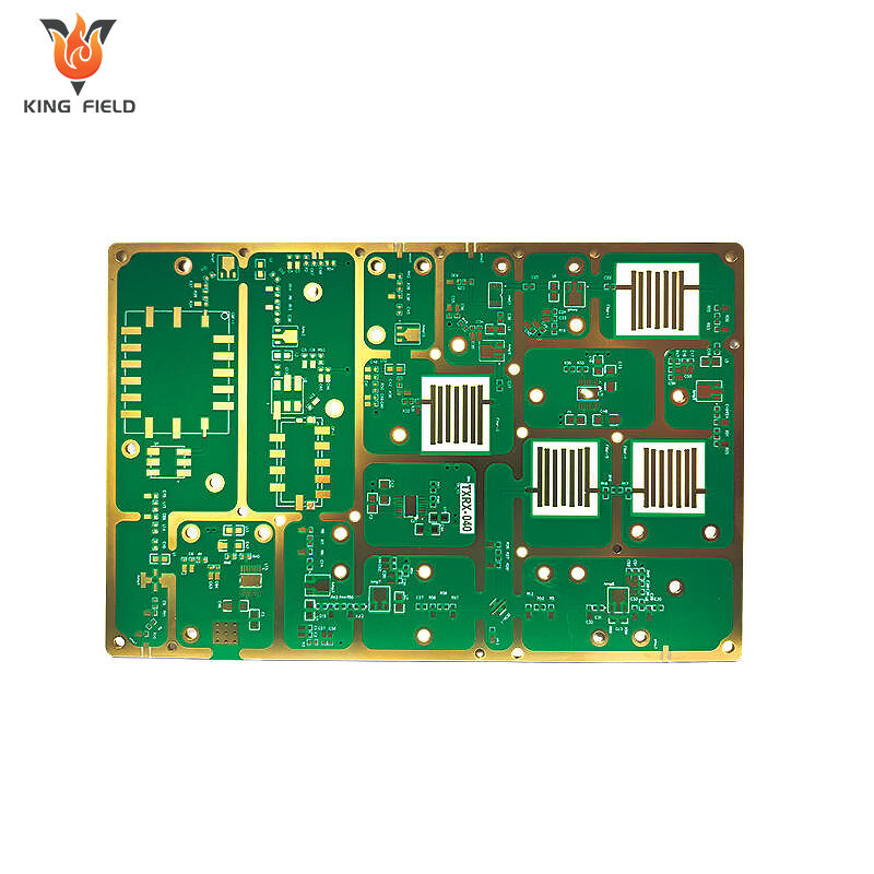
A PCB is the fundamental building block of modern electronic circuits. At its core, a Printed Circuit Board is a thin board—usually made of a non-conductive substrate—overlaid with thin layers of conductive copper. These copper layers are etched to create intricate patterns called traces, which serve as electrical pathways connecting various electronic components such as resistors, capacitors, integrated circuits (ICs), and connectors. Simply put, a PCB allows electronic signals and power to travel between components efficiently and reliably, all within a compact, organized, and manufacturable design.
Substrate/Base Material The majority of PCBs use FR-4, a fiberglass-reinforced epoxy laminate known for its excellent mechanical stability and electrical insulation. Flex and rigid-flex PCBs may use polyimide or other materials to allow bending and folding.
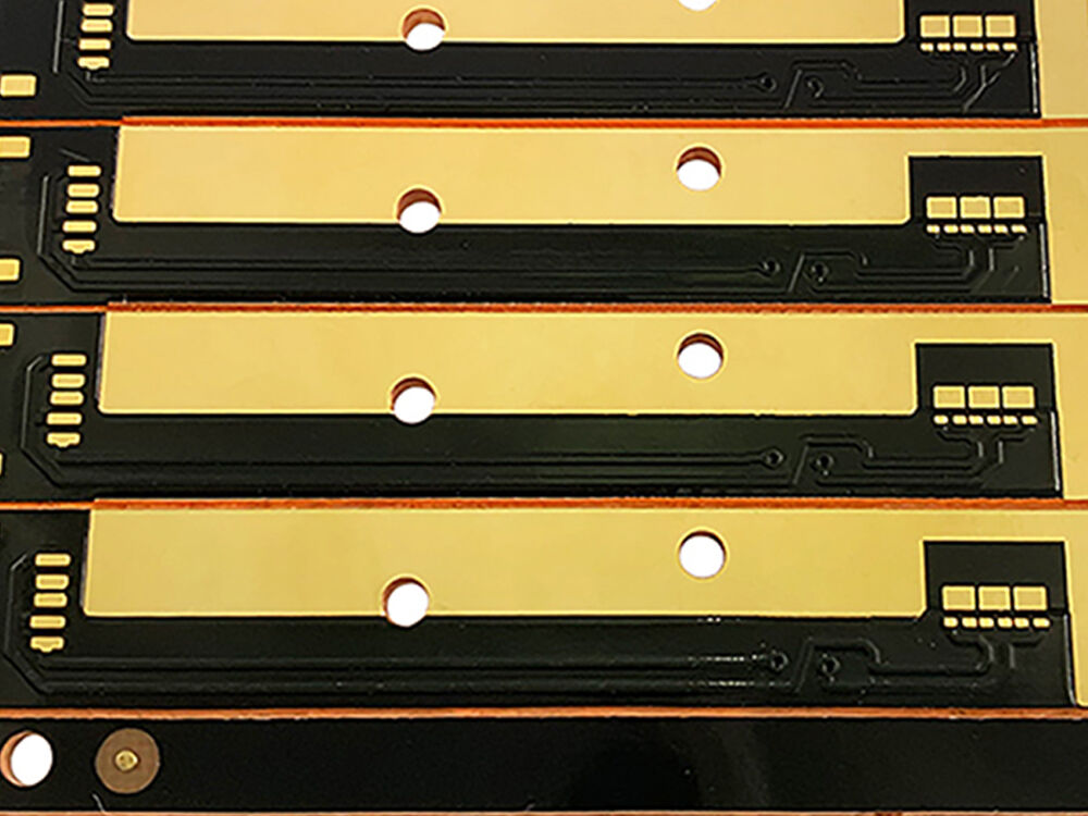
Copper Layers Every circuit board contains at least one layer of copper, laminated tightly against the substrate. Single-sided PCBs have one copper layer, while multilayer PCBs can have up to 30 or more, enabling highly dense and sophisticated circuit designs. These layers form the traces and pads that define electrical connections.
Solder Mask This green insulating layer is applied over the copper to protect it from oxidation and prevent accidental solder bridges during the PCB assembly process. Openings in the mask expose only necessary pads for soldering electronic components.
Silkscreen Layer Using a special ink, this layer prints reference labels, logos, polarity marks, and other information directly onto the circuit board surface, aiding assembly, testing, and troubleshooting.
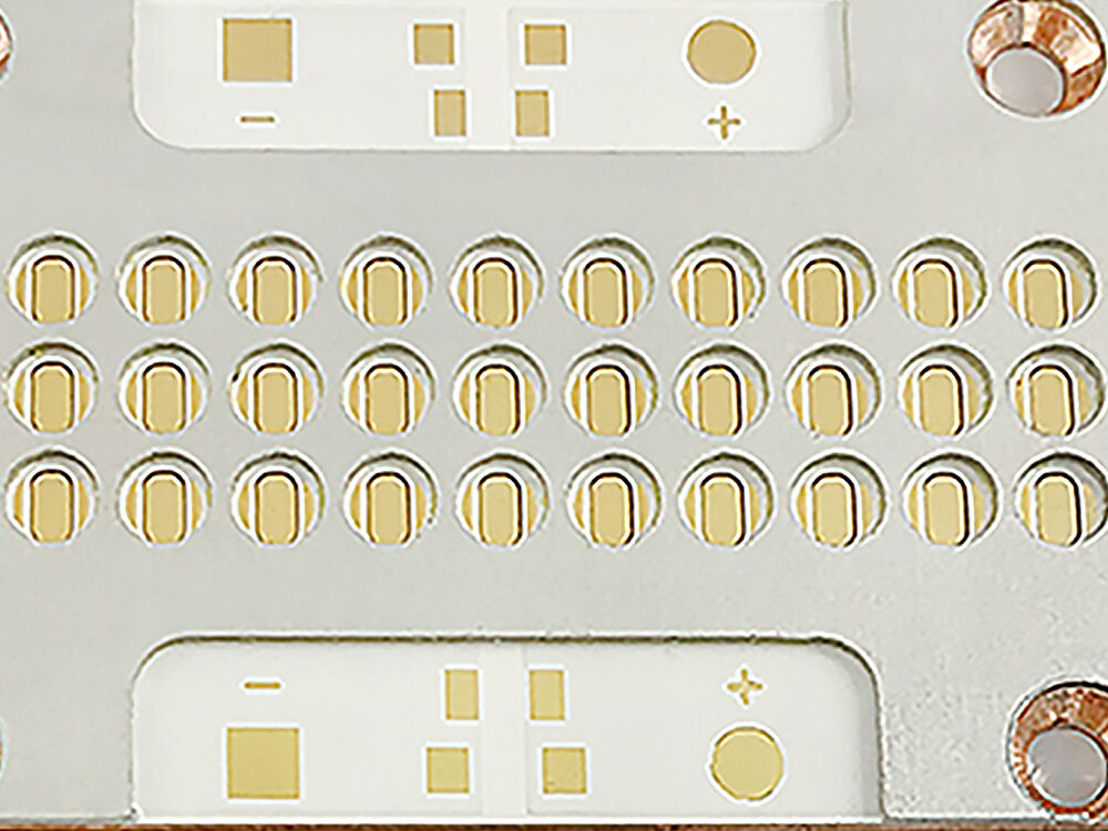
Vias and Plated Through Holes (PTH) Vias are tiny holes drilled and plated with copper, allowing connections between copper layers. Through-hole vias pass through all layers, while blind and buried vias connect specific internal layers in complex, high-density boards.
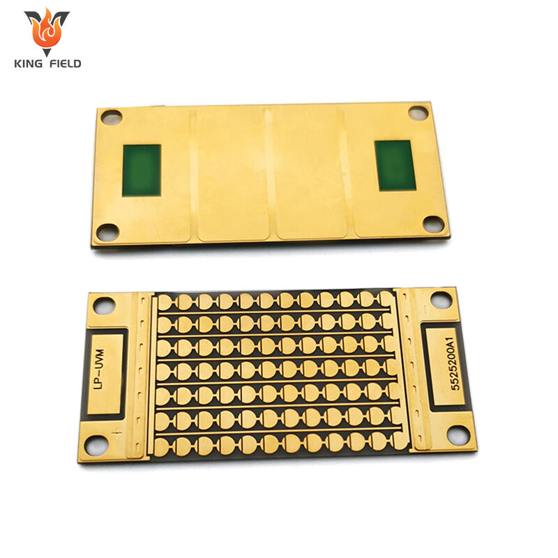
Edge Connectors These are gold-plated copper pads along the board's edge, providing an interface for plug-in modules or direct slot insertion—common in memory modules and expansion cards.
|
PCB Feature |
Function |
|
FR-4 Substrate |
Mechanical rigidity, insulation |
|
Copper Layers |
Signal and power traces, ground planes |
|
Solder Mask |
Prevents oxidation and solder shorts |
|
Silkscreen |
Component labeling, assembly guidance |
|
Vias/PTH |
Inter-layer signal/power connections |
|
Edge Connectors |
Interface with other system components |
There are many PCB types tailored for specific application needs:
In a basic digital thermostat, a single-sided PCB reduces costs and speeds up manufacturing since the circuit is simple and there are no high-speed signals. Conversely, a smartphone motherboard must use a multilayer PCB: the dense arrangement of ICs and high-speed data signaling can only be achieved by stacking many layers together, carefully managing signal integrity and impedance control.
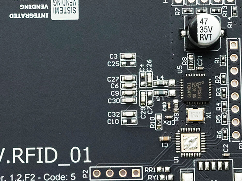
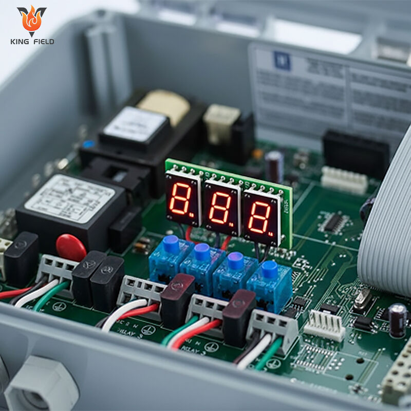
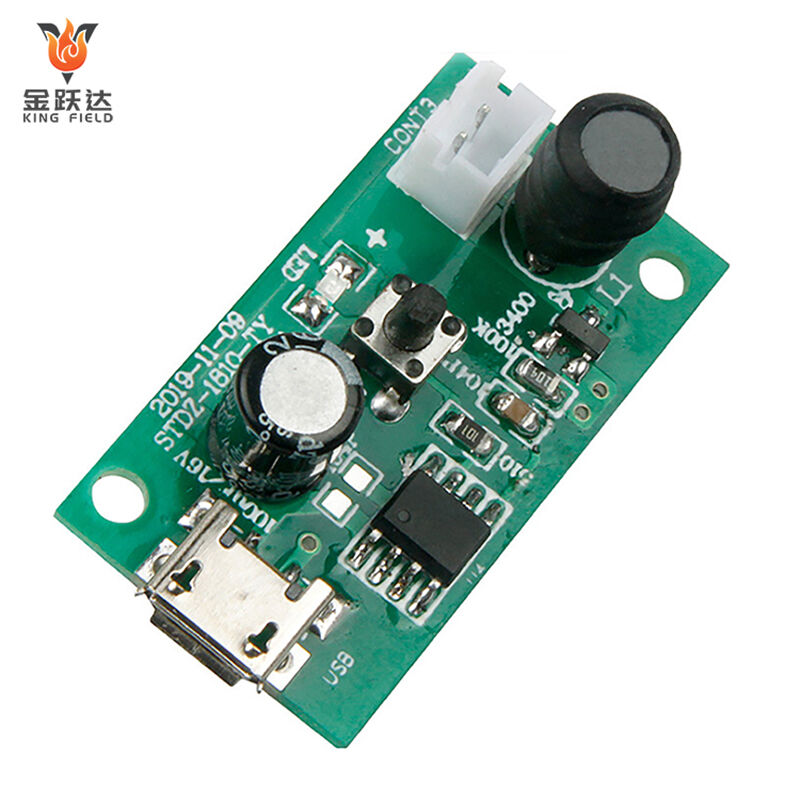
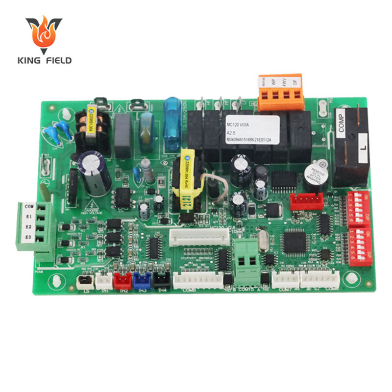
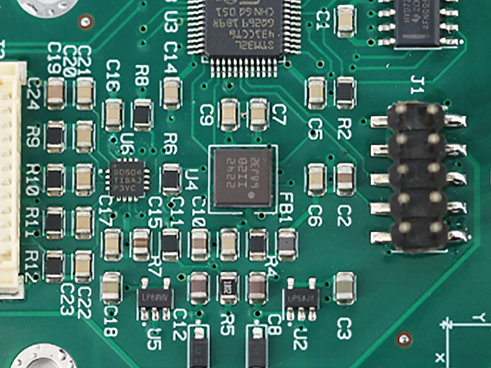
A PCBA (Printed Circuit Board Assembly) is the next step in the journey from raw design to functional electronics. If the PCB (Printed Circuit Board) is the blank canvas, then the PCBA is the finished masterpiece—populated with electronic components that, together, form a working electronic circuit.
In essence, PCBA refers to a PCB that has undergone the full assembly process: all passive and active electronic components—such as resistors, capacitors, diodes, transistors, and complex integrated circuits (ICs)—are precisely mounted and soldered onto the board according to the circuit design. Only after this assembly does the board become a functional system, capable of carrying out its intended purpose, whether that’s regulating power in an industrial drive, managing signals in a communication device, or running a sophisticated microcontroller in an IoT gadget.
The PCBA is more than just a sum of its parts; it is the seamless integration of mechanical, electrical, and materials engineering. Here’s what makes up a standard PCBA:
There are two principal technologies used in the assembly of PCBAs: Surface-Mount Technology (SMT) and Through-Hole Technology (THT). In some advanced assemblies, these methods are combined, especially for prototype assembly or where both mechanical strength and high component density are required.
SMT is the dominant PCB assembly method for modern electronics. Instead of inserting component leads through holes, components are mounted directly onto the surface of the PCB onto specialized pads.
Advantages of SMT include:
SMT is ideal for:
Key Steps in SMT Assembly:
THT involves inserting component leads through drilled holes in the PCB and soldering them on the opposite side, typically by wave soldering or manual techniques.
Advantages of THT:
THT is common in:
THT Assembly Process:
|
Aspect |
Surface-Mount Technology (SMT) |
Through-Hole Technology (THT) |
|
Component Size |
Very small (SMD components) |
Larger (axial, radial, DIP, etc.) |
|
Placement |
On board surface |
Through drilled holes |
|
Automation |
Fully automated, high-speed |
Manual or semi-automated |
|
Mechanical Strength |
Moderate (enhanced in some packages) |
High, ideal for stressed components |
|
Main Use |
Modern, high-density, compact electronics |
Ruggedized, high-power, legacy designs |
A completed PCBA undergoes comprehensive PCBA testing before shipment, ensuring that all electrical and functional requirements are met. This includes In-Circuit Testing (ICT), Functional Circuit Testing (FCT), and increasingly advanced methods like Automated Optical Inspection (AOI) and X-ray for critical assemblies such as BGA (Ball Grid Array) and LGA parts.
The relationship between PCB (Printed Circuit Board) and PCBA (Printed Circuit Board Assembly) is at the heart of modern electronics manufacturing. Understanding this connection is essential for product designers, procurement professionals, and electronics engineers who need to move from concept to reality in the most efficient way possible.
|
Stage |
Description |
Outcome |
|
PCB Design & Fabrication |
Board layout, etching, drilling, plating |
Bare PCB |
|
Parts Procurement |
Ordering and preparing components |
Unpopulated board + loose parts |
|
Assembly & Soldering |
Solder paste, pick-and-place, reflow/wave soldering |
Soldered, populated completed PCBA |
|
Testing & Inspection |
ICT, FCT, AOI, X-ray |
Verified, functionally ready PCBA |
PCB is essential for early prototyping and design validation, allowing engineers to test layouts and high-speed routing before committing to component assembly.
ICT (In-Circuit Test): Probes test electrical properties, checking solder integrity, shorts, opens, and basic device functionality.
FCT (Functional Test): Simulates the PCB’s real-world operating environment, verifying firmware, communication, and full circuit function.
Flying Probe Test: Needle probes move rapidly across the board, testing open/shorts without a custom fixture—a cost-effective solution for prototypes and low-volume runs.
AOI & X-ray: Inspects solder joints under BGA/chip-scale packages invisible to standard cameras.
Aging/Burn-in Test: Stresses the PCBA at elevated voltages and temperatures, detecting early-life failures and establishing reliability metrics.PCBA is crucial for functional testing, product shipment, and customer delivery, tying the electrical, mechanical, and manufacturing disciplines into a streamlined process.
The PCB manufacturing process is a sequence of highly controlled steps that turns an electronic schematic into a tangible, precise, and robust platform for building today’s electronic marvels. Whether ordering a PCB prototype or preparing for mass production, success starts with understanding this process in detail.
Every PCB project begins with PCB design using specialized CAD software. Engineers lay out the board, defining the routing of traces and the placement for all components, vias, and pads. Aspects such as trace width, spacing, and copper layer count are specified according to electrical performance, thermal requirements, and mechanical constraints. To ensure consistency with advanced PCB assembly processes, proper DFM (Design for Manufacturability) practices must be followed, such as ample pad sizes, clear silkscreen markings, and well-defined keepout zones.
The result is an essential set of manufacturing files:
Fact: “A single error in a Gerber file can halt a multi-million-dollar production run and compromise product reliability.”
The PCB substrate—often FR-4 for rigid boards or polyimide for flex circuits—is prepared in large sheets.
This stage creates the intricate circuit patterns:
Modern PCBs rely on sophisticated layer interconnections:
Next, the familiar green (or sometimes blue, red, or black) solder mask is applied:
A vital step for assembly and service, the silkscreen layer uses non-conductive ink to print labels, polarity marks, logos, and other identifiers:
All exposed copper pads must be protected and prepared for soldering:
Before any board moves to the PCB assembly process:
|
Step |
Details/Tools Used |
Importance |
|
1. PCB Design |
CAD software, Gerber files |
Blueprint for all fabrication |
|
2. Substrate Prep |
FR-4/polyimide laminates, copper cladding |
Mechanical and insulative backbone |
|
3. Patterning/Etching |
Photoresist, UV exposure, chemical etching |
Creates circuit pathways |
|
4. Drilling/Plating |
CNC drills, plating baths |
Inter-layer connections |
|
5. Solder Mask |
Liquid mask, UV curing |
Insulation, prevents shorts |
|
6. Silkscreen |
Screen printer, ink |
Component ID/assembly aid |
|
7. Surface Finish |
HASL, ENIG, OSP, electroplating |
Soldering efficiency, longevity |
|
8. Testing/Inspection |
Flying probe, AOI, QC tools |
Ensures manufactured quality |
Professional PCB fabrication services minimize defects, enable quick turn PCB production, and offer high consistency for large or low volume PCB orders. By leveraging advanced equipment and controls, manufacturers achieve not only dimensional accuracy but also electrical reliability critical in aerospace, medical devices, and automotive electronics.
After PCB manufacturing delivers the blank circuit board, the next crucial stage is the PCB assembly process (PCBA process), which transforms the inert PCB into a functional printed circuit board assembly (PCBA). This phase is where the design truly comes to life as electronic components are placed, joined, and tested to create a working circuit capable of powering everything from consumer gadgets to high-reliability aerospace systems.
Efficient PCBA assembly starts with precise data and reliable materials:
SMT assembly dominates modern PCBA thanks to its speed, miniaturization, and compatibility with automation.
Solder Paste Application: A stainless steel stencil aligns over the PCB, and solder paste—a mixture of microscopic solder balls suspended in flux—is squeegeed across, filling the exposed component pads.
Automated Pick-and-Place: High-speed robotic arms equipped with vision systems pick tiny SMD (Surface-Mount Devices)—like microchips, resistors, and capacitors—from reels or trays and place them on the pasted pads, following the centroid data.
Reflow Soldering: The populated PCB enters a multi-zone reflow oven. Carefully controlled temperature profiles melt the solder paste, which then cools and solidifies, forming robust electrical and mechanical connections between component leads and copper pads.
Automated Optical Inspection (AOI): High-resolution cameras scan each board, comparing actual component placement and solder joint quality against the design files. This catches misalignments, tombstoning, voids, and shorts before assembly proceeds.
|
Step |
Purpose |
|
Solder Paste Printing |
Applies solder only to component pads |
|
Pick-and-Place |
Automated precise placement of all SMDs |
|
Reflow Soldering |
Solidifies connections, ensures reliability |
|
AOI |
Catches defects quickly and accurately |
Large connectors, power components, transformers, and parts needing extra strength use THT assembly. This process involves:
Component Insertion: Operators (or robots) insert component leads into plated through holes (PTHs), ensuring proper orientation and placement against the silkscreen.
Wave Soldering: The board travels across a molten solder “wave” that instantly forms hundreds of high-strength joints on the solder side. For sensitive or complex assemblies, selective soldering and manual touch-up are also common.
Lead Trimming and Cleaning: Excess leads protruding through the board are trimmed. Boards are washed to remove flux and residues, securing long-term performance and insulation resistance.
Modern boards often require both SMT and THT techniques. For example, a power supply PCBA might use SMT for signal processing ICs and THT for high-current terminals. This mixed approach maximizes electrical performance and mechanical durability.
Professional PCB assembly always ends with rigorous testing and inspection to guarantee reliability—especially crucial for medical devices, automotive electronics, and aerospace PCBs.
Choosing the right partner for your PCB (Printed Circuit Board) manufacturing or PCBA (Printed Circuit Board Assembly) needs is one of the most important decisions in the electronics product lifecycle. Your contract manufacturer's skill, process quality, and service excellence directly affect your circuit board’s performance, your development speed, your cost competitiveness—and ultimately, your success in the market.
Whether you require rapid prototyping, complex multilayer stackups, or turnkey assembly for demanding applications, a trustworthy PCB/PCBA supplier must provide more than just good pricing. Here’s what you should look for:
A proven track record in your application sector is critical. Medical devices, automotive ECUs, aerospace electronics, consumer gadgets, and industrial controls all have different requirements for compliance, documentation, and tolerances. Look for:
Trustworthy PCB/PCBA manufacturers follow international standards to guarantee performance, reliability, and traceability. Insist on:
Leading-edge PCB and PCBA partners offer advanced manufacturing techniques:
Exceptional manufacturers add value before a single board is built:
Quality assurance isn’t just a checkbox—your supplier must offer multi-stage inspections for both boards and assembled units:
Delays and defects often arise from component shortages or counterfeits. Reliable manufacturers:
|
Selection Factor |
What To Check |
Why It Matters |
|
Industry Experience |
Relevant case studies, references |
Trust and application fit |
|
Certifications |
ISO, IPC, UL, RoHS, etc. |
Compliance and reliability |
|
Capabilities |
Multilayer, flex, HDI, BGA, volume, quick turn |
Flexibility for project growth |
|
DFM/Engineering Support |
Free DFM, layout review |
Fewer errors, higher yields |
|
Quality/Inspection |
AOI, X-ray, test types, batch traceability |
Defect minimization, data-driven |
|
Supply Chain |
Authorized parts, supply chain management |
Avoid delays/counterfeits |
|
Service & Cost |
Lead time, clear pricing, support |
Schedule and budget reliability |
As a trusted partner in the electronics industry, we understand that seamless integration of PCB manufacturing and PCB assembly services is essential for success, whether you’re developing a quick-turn prototype or scaling to high-volume production. Our offerings are rooted in state-of-the-art technology, rigorous quality standards, and deep industry experience, enabling you to bring your electronic innovations to life efficiently and reliably.
Our capabilities extend across the complete PCB and PCBA value chain:
|
Service |
Description & Benefits |
|
PCB Manufacturing |
Multilayer, flex, rigid-flex, specialty materials, fast prototype |
|
PCB Design & DFM |
Stackup, impedance, manufacturability checks, design optimization |
|
SMT & THT Assembly |
Automated lines, BGA, QFN, precision soldering |
|
AOI & X-ray Inspection |
Detect hidden defects, ensure zero faults |
|
Functional & ICT Testing |
Application-level, boundary scan, flying probe |
|
R&D & Engineering |
Prototyping, small batch, custom project development |
|
Intelligent Management |
MES, ERP, CRM, barcode tracking, real-time order monitoring |
|
Industry Specialization |
Medical, automotive, industrial, power, consumer, aerospace |
Q1: What is the main difference between PCB and PCBA?
A: A PCB is a bare board made of insulating substrate (usually FR - 4) with copper traces, solder mask, and silkscreen, serving as the mechanical and electrical base. A PCBA is a functional, tested assembly where electronic components (resistors, capacitors, ICs, etc.) are placed and soldered onto the PCB.
Q2: Which is more expensive—PCB or PCBA?
A: PCBA is more expensive. Its cost includes the PCB itself, electronic components, assembly labor, testing, supply chain management, and quality control.
Q3: What are the most common PCB surface finishes, and how do they affect PCBA?
A: Common surface finishes and their impacts:
HASL: Cost - effective, suitable for THT assembly.
ENIG: Flat, oxidation - resistant, ideal for SMT and fine - pitch/BGA components.
OSP: Simple, eco - friendly, for short - term use.
Hard Gold: Used for edge connectors ("gold fingers").
Q4: What types of PCB testing are typically done for PCBA?
A: Common PCBA testing methods:
ICT: Checks component placement, solder joints, and common faults.
FCT: Tests circuits under simulated operating conditions.
AOI: Ensures component placement, orientation, and solder quality.
X - ray Inspection: For BGAs, CSP, QFN, and hidden joints.
Flying Probe Test: Fits prototypes/low - volume runs (no custom fixtures needed).
Burn - in/Aging Test: Stresses mission - critical PCBs to eliminate early failures.
Q5: What industries require the highest standards for PCB and PCBA?
A: Medical devices, automotive & EV, aerospace & defense, telecommunications, industrial controls.
Understanding PCB and PCBA differences goes beyond industry terminology—it masters the core processes of all electronic devices (from consumer gadgets to aerospace modules). This knowledge helps engineers, startups, and manufacturers confidently handle design, sourcing, prototyping, and production.
 Hot News
2026-01-17
2026-01-16
2026-01-15
2026-01-14
2026-01-13
2026-01-12
2026-01-09
2026-01-08