Quick Links
Successful PCB assembly is a meticulously orchestrated operation that turns a bare printed circuit board—fabricated according to your exact PCB design—into a completed, functional hardware product. This process is the heart of electronic manufacturing, spanning from preparatory checks on your design files to quality testing of the finished assembled board. Here’s a detailed look at every major stage of the PCB assembly process flow, incorporating both Surface Mount Technology (SMT) and Through-Hole Technology (THT) elements.
Before a single component is placed or soldered, expert assembly partners start with a DFA (Design for Assembly) check. This review is crucial for smooth, error-free PCBA:
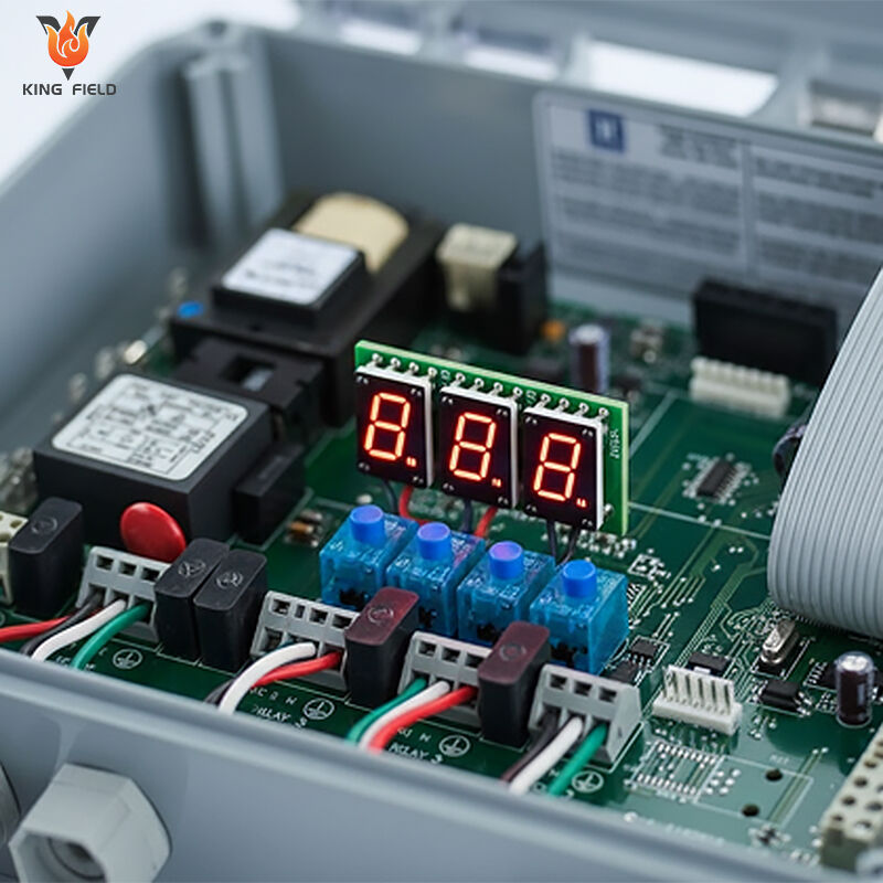
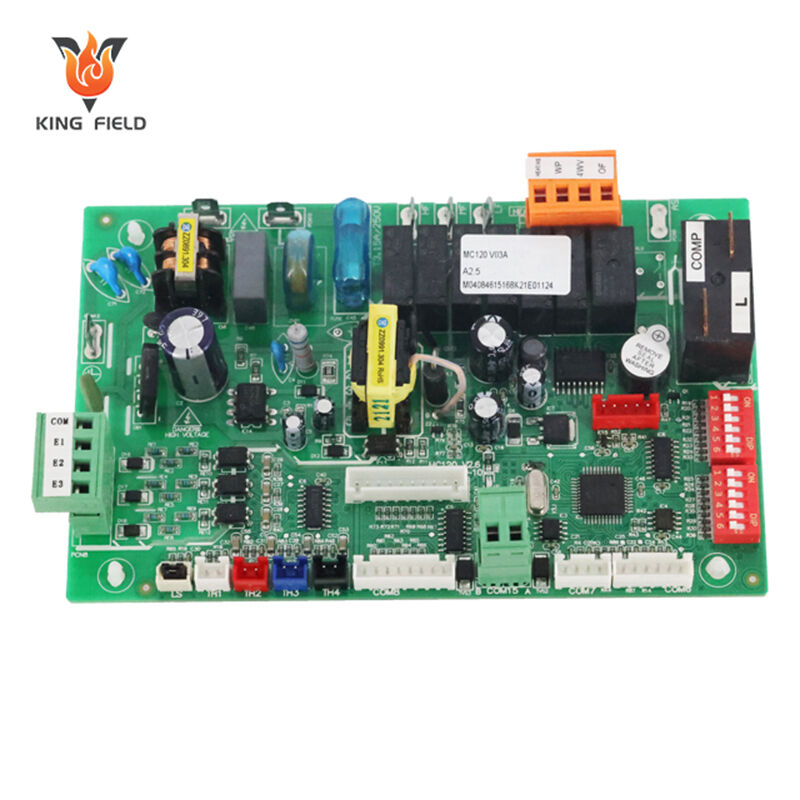
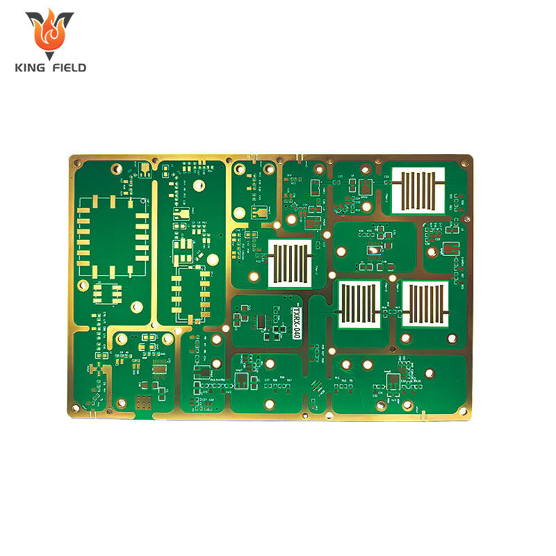
SMT assembly is the fastest and most automated part of PCB assembly, enabling high-density, cost-effective placement of surface-mount devices (SMDs).
The process starts with the precise application of solder paste—a blend of ultra-fine solder powder and flux—onto the PCB pads.
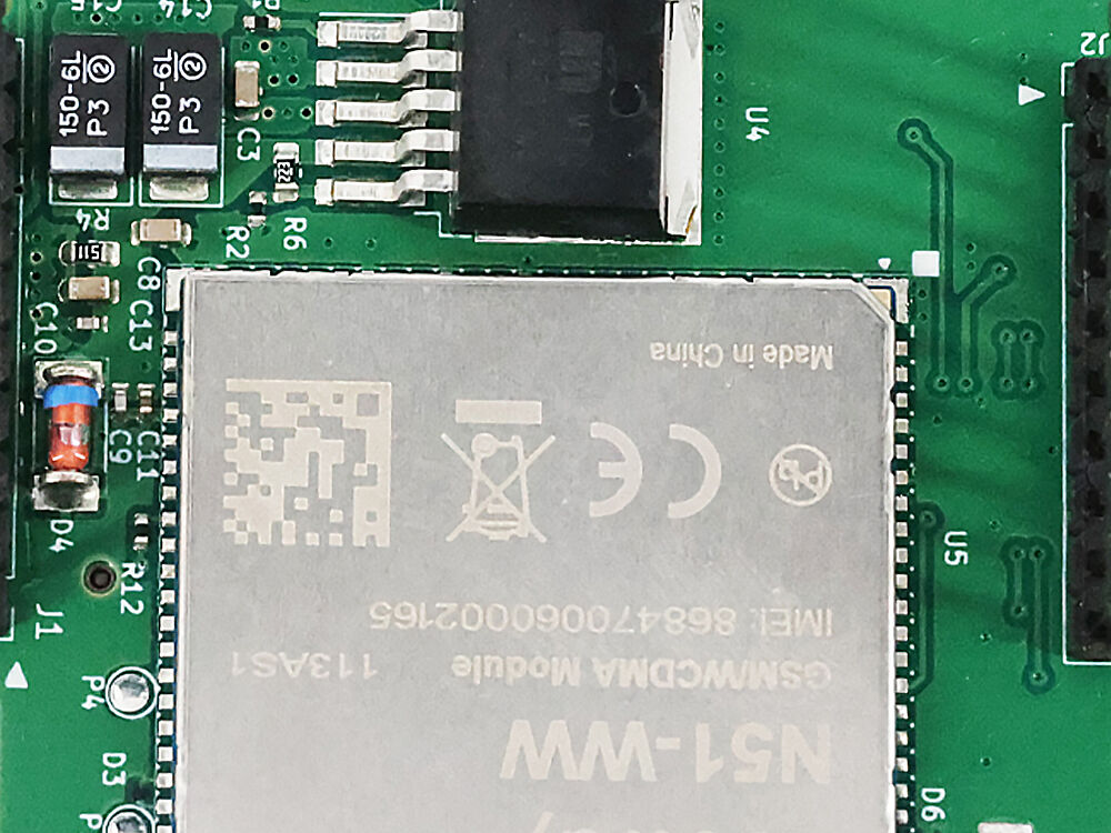
With the solder paste in place, advanced pick and place machines accurately position SMD chips, resistors, capacitors, ICs (including BGAs and QFNs), and other devices onto the board.
The populated board is then sent through a reflow oven:
AOI systems take high-resolution images of the reflowed board to check for defects such as:
Automated inspection dramatically increases yield by catching issues early, allowing for rapid correction.
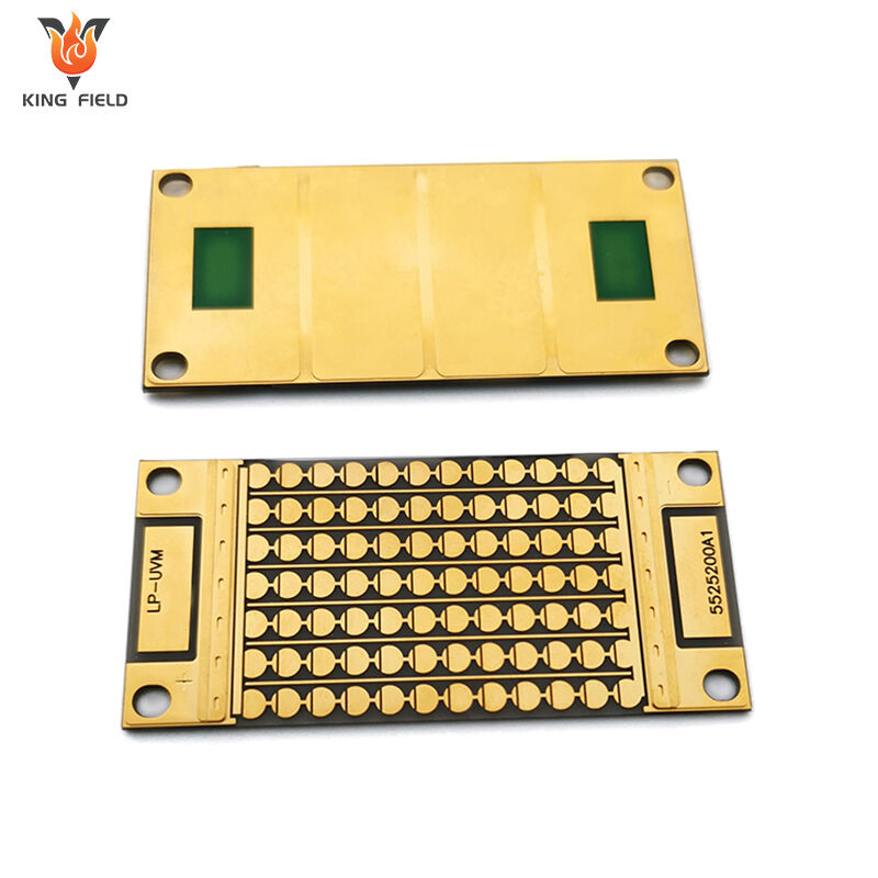
X-ray inspection is critical for BGA (Ball Grid Array), micro-BGA, and other parts where solder joints are hidden. This process reveals:
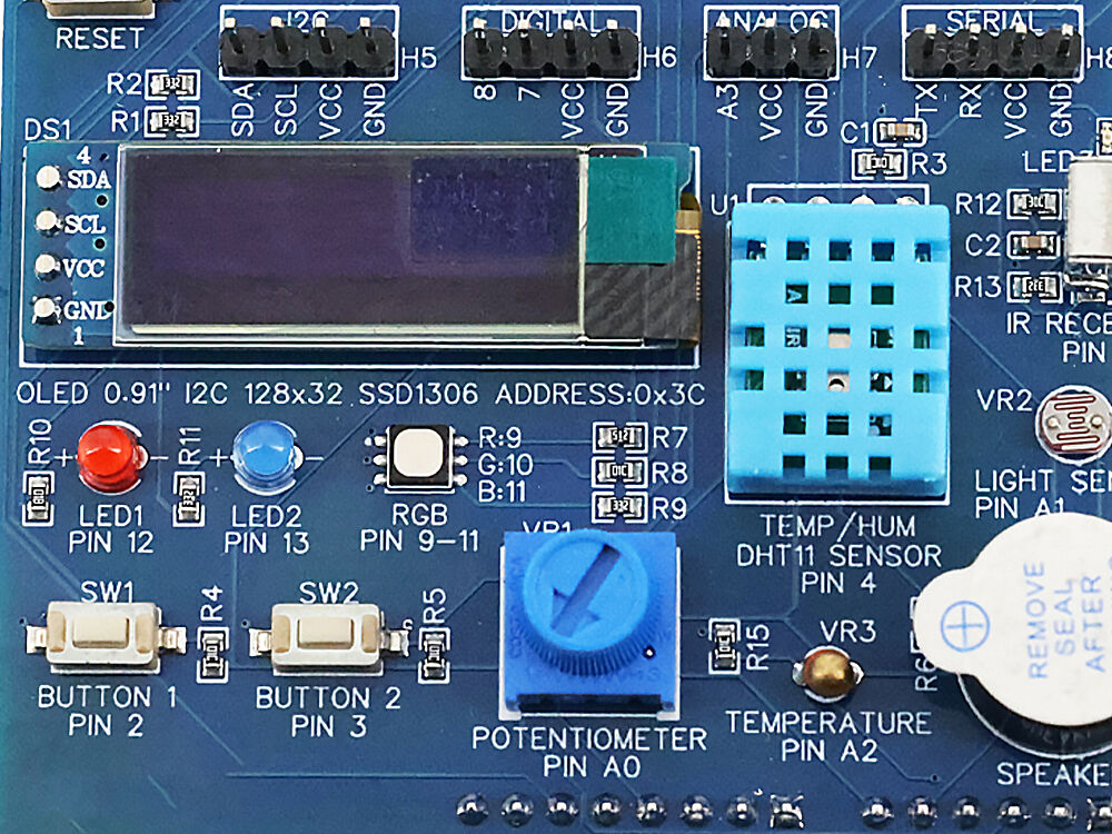
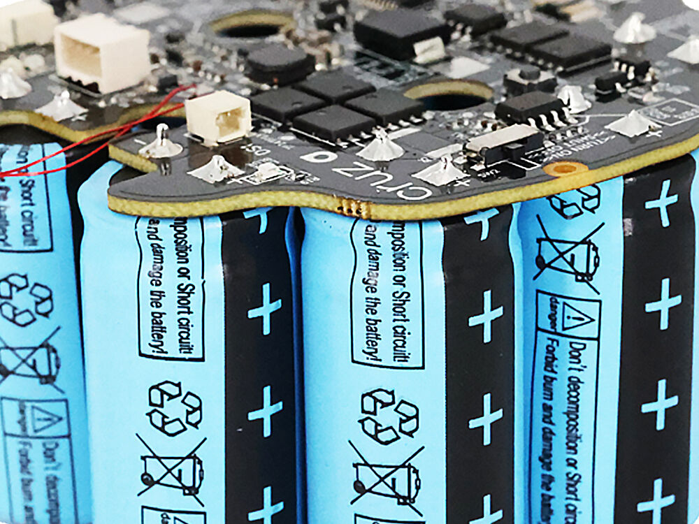
Although SMT dominates, many boards include through-hole components for connectors, large capacitors, or high-mechanical-stress elements.
After soldering, boards are cleaned to remove flux residue—unless no-clean flux is specified, in which case residue is safe to leave on.
For sensitive or non-washable component types, special soldering techniques and fluxes are used that don't require further cleaning.
|
Inspection/Test Type |
What It Detects |
Application |
|
AOI |
Soldering defects, misalignments, missing/extra parts |
All assembly, post-reflow |
|
X-ray |
Internal BGA defects, hidden solder joints, voids |
High-density, BGA, micro-BGA |
|
FPT (Flying Probe) |
Open circuits, short circuits, basic function |
Prototype, low-volume |
|
ICT/Functional |
Complete operational check, electrical values, firmware |
Mass production, QA |
Boards destined for harsh or moisture-prone environments often undergo conformal coating:
Final tested and coated boards are labeled, serialized, kitted, and carefully packaged according to type and regulatory requirements—ready for integration, large-scale deployment, or direct shipment to end users.
In summary: The modern PCB assembly process is a precise, multi-stage journey from data validation and DFA/DFM checks, through SMT and THT assembly, automated and manual inspections, to advanced electrical testing, coating, and shipment. Each step is designed to maximize electrical performance, reliability, and manufacturability for every PCBA—whether you're building rapid PCB prototypes or scaling to high-volume production.
Surface Mount Assembly (SMA) is a core PCBA process for medical, automotive, industrial control, and consumer electronics. It uses surface mount devices (SMDs) attached directly to PCB surface pads, enabling miniaturization, high component density, and automated mass production, complying with IPC-A-610 and IPC-J-STD-001 standards.
Pre-Production Preparation & PCB Pre-Conditioning: Verify CAD design for SMD compatibility; inspect incoming PCBs (no warpage, clean pads) and SMDs (authenticity, no damage); bake high-Tg FR4 PCBs (125°C, 4–8h) and store moisture-sensitive SMDs in dry cabinets to prevent soldering defects.
Solder Paste Printing: Use a stencil to deposit solder paste on pads; control stencil thickness (0.12–0.15mm), squeegee pressure (15–25N), and speed (20–50mm/s); adopt 3D SPI for fine-pitch components to check paste volume and shape.
SMD Placement: High-speed pick-and-place machines with CCD cameras place components (±0.03mm precision). High-speed for passives (up to 100,000/hour), precision placement for ICs/sensors; use ESD protection and force calibration for sensitive automotive/medical components.
Reflow Soldering: RoHS-compliant SAC305 solder undergoes a 4-stage oven profile: preheat (150–180°C), soak (180–200°C, 60–90s), reflow (peak 245–260°C, 10–20s), cooling (2–4°C/s). Adjust cooling rates for high-Tg FR4 PCBs to reduce thermal stress.
Post-Reflow Inspection (PRI): AOI detects bridges, cold joints, tombstoning; X-ray inspects hidden BGA/CSP joints for voids. 100% inspection for medical/automotive PCBs, sampling for consumer electronics.
Rework & Touch-Up: Correct defects with soldering irons/hot air stations; replace damaged components; clean flux residue with isopropyl alcohol; document rework for high-value PCBs.
Conformal Coating (Optional): Apply acrylic/silicone/urethane coating via spraying/dipping for harsh environments (automotive engine compartments, industrial floors). Use biocompatible coatings for medical PCBs.
Final Functional Testing & QA: Conduct operational tests (sensor output, communication modules, signal integrity); perform dimensional and continuity checks; package qualified PCBs in anti-static/moisture barrier bags.
 Hot News
2026-01-17
2026-01-16
2026-01-15
2026-01-14
2026-01-13
2026-01-12
2026-01-09
2026-01-08