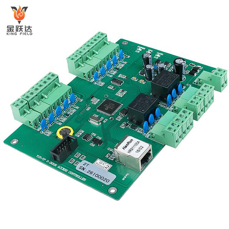
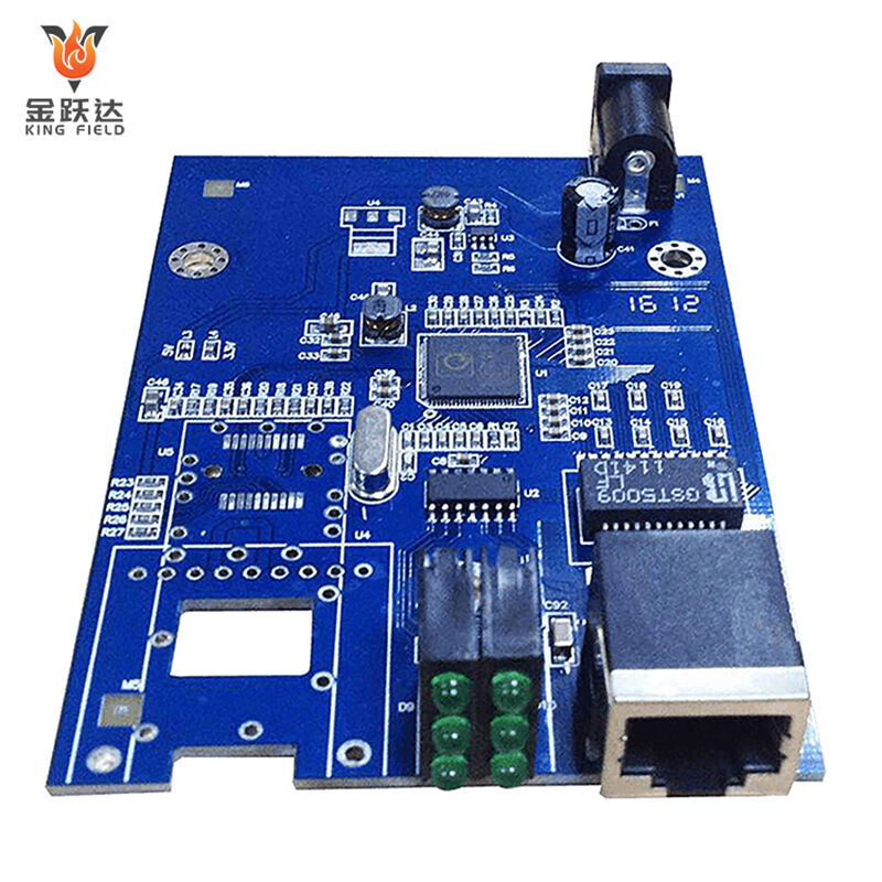
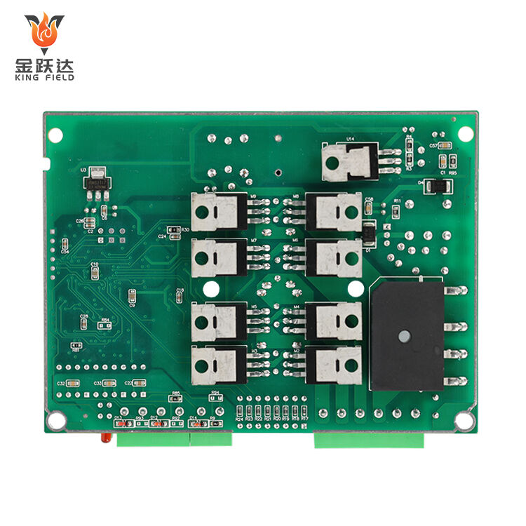
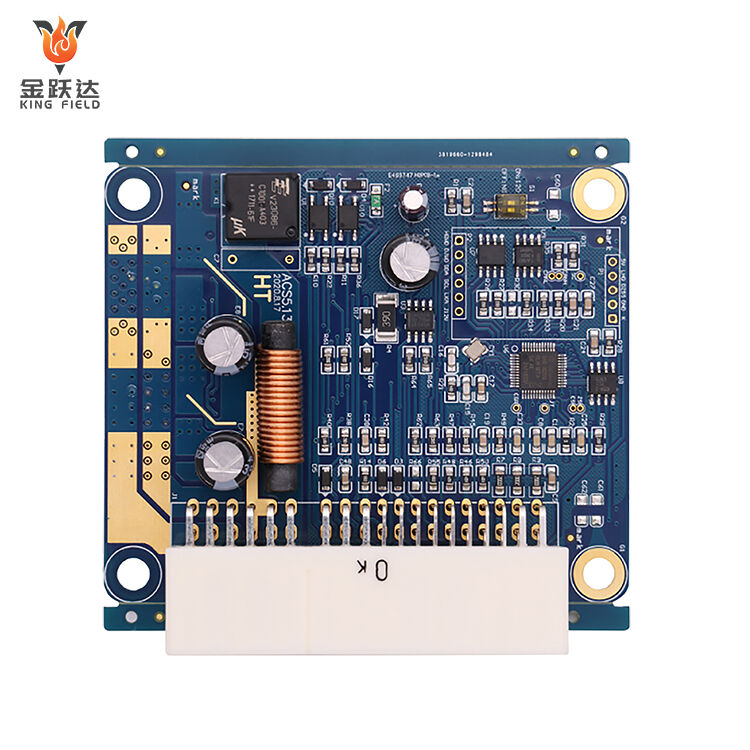
SMT Assembly
Precision SMT Assembly for medical, industrial, automotive & consumer electronics. Fast prototyping (24h) to mass production, BOM matching, DFM analysis & AOI/ICT testing. High-speed placement, reliable soldering—on-time delivery, consistent quality for your PCBs.
Description
Precision SMT Assembly Solutions
KING FIELD provides high-quality, reliable surface mount technology assembly services for your electronics manufacturing needs.
Regarding KINGFIELD SMT Assembly
KING FIELD is a leading surface mount technology (SMT) assembly service provider, offering high-quality manufacturing solutions to electronics companies worldwide.
Our capabilities
- High-speed SMT placement (up to 80,000 components per hour)
- Component sizes from 01005 to large BGAs
- Double-sided placement capability
- Automated Optical Inspection (AOI) and X-ray inspection
- Flexible production from prototyping to high-volume manufacturing
- One-stop PCBA solution for your ideas
- Over 10 years of trusted PCBA manufacturing expertise
- 9 automated SMT production lines for delivery
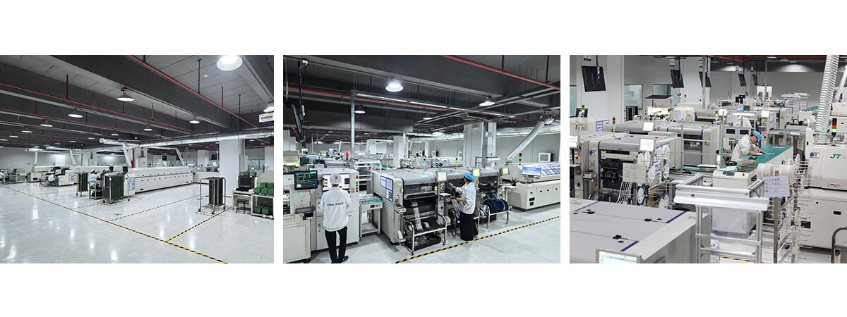
Advanced manufacturing
We are equipped with state-of-the-art SMT production lines to provide precision assembly with high efficiency and reliability.
Quality assurance
Our rigorous processes are certified to ISO 9001, IATF 16949, and ISO 13485 standards, ensuring consistent quality for every project.
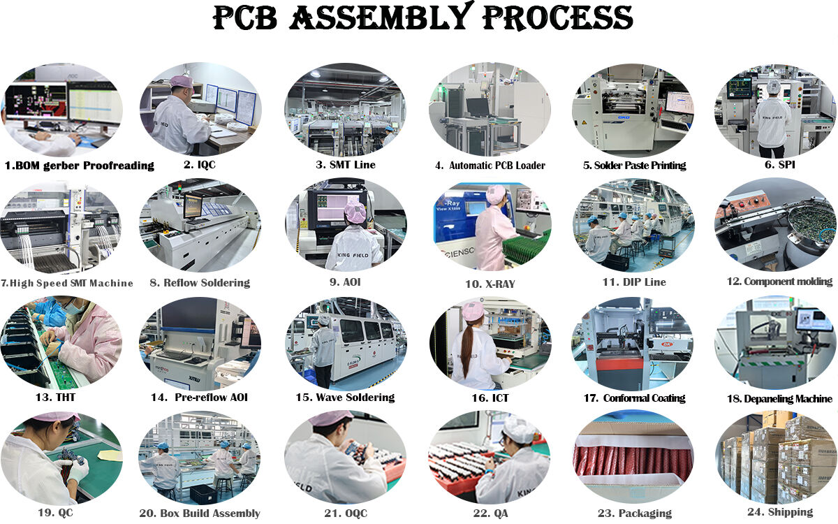
Surface mount technology (SMD) assembly is a core process in current electronic product manufacturing. It refers to the direct application of solder paste to designated pads on the surface of a printed circuit board (PCB) to form leadless or short-lead miniature surface mount components, followed by high-temperature reflow soldering to secure them. This differs from traditional through-hole mounting technology, which requires drilling holes in the PCB. The process relies on three core elements: SMD components, solder paste printers/pick-and-place machines/reflow ovens, and dedicated PCBs. A typical workflow consists of four key steps: solder paste printing, component placement, reflow soldering, and inspection and rework (AOI inspection and repair of defective products), ultimately forming a complete and stable electronic circuit.
Advantages of SMT assembly
-
Significantly Reduced Product Size and Weight:
Components can be directly mounted on the PCB (Printed Circuit Board) surface without through-holes, saving the installation space required for traditional through-hole components. For the same function, products using SMT can be more than 60% smaller and more than 70% lighter, meeting the miniaturization needs of portable devices such as mobile phones and laptops.
-
Increased Production Efficiency and Reduced Costs:
High automation allows for high-speed, high-precision batch mounting via pick-and-place machines. A single production line can assemble tens of thousands of PCBs per day. Material utilization is higher; smaller components with no leads reduce material waste; the production process is simplified, and labor costs are reduced.
-
Enhanced Circuit Performance and Reliability:
Components are mounted more securely, with shorter solder joint distances and straighter paths, reducing signal transmission delays and interference, and improving the performance of high-frequency circuits. The solder joint defect rate is low, and contact problems caused by vibration and temperature changes in through-hole components are avoided, significantly improving overall product reliability.
-
High-Density SMT Assembly:
With technological advancements, electronic products are becoming increasingly intelligent and sophisticated, necessitating a significant increase in PCB assembly density. SMT assembly effectively addresses this issue, making high-density PCB assembly possible.
SMT assembly process flow
Equipment parameters
| Equipment manufacturing process capability | |
| SMT Capacity | 60,000,000 chips/day |
| THT Capacity | 1.500,000 chips/day |
| Delivery Time | Expedited 24 hours |
| Types of PCBs Available for Assembly | Rigid boards, flexible boards, rigid-flex boards, aluminum boards |
| PCB Specifications for Assembly |
Maximum size: 480x510 mm; Minimum size: 50x100 mm |
| Minimum Assembly Component | 01005 |
| Minimum BGA | Rigid boards 0.3 mm; Flexible boards 0.4 mm |
| Minimum Fine-Pitch Component | 0.2 mm |
| Component Placement Accuracy | ±0.015 mm |
| Maximum Component Height | 25 mm |
Common problems in SMT assembly
-
Solder Paste Related Issues:
Excessive solder paste can cause short circuits between adjacent solder joints, while insufficient paste results in weak solder joints (cold solder joints).
Improper storage, warming, or use beyond the expiration date of the solder paste can lead to deterioration, resulting in bubbles and dull solder joints after soldering.
Inaccurate positioning by the printing press can cause solder paste to shift off the PCB pads, affecting subsequent component placement.
-
Component Placement Issues:
Visual errors in the pick-and-place machine or wear on the nozzle can cause component placement misalignment, leading to poor soldering or contact problems.
Incorrect material loading or nozzle failure can result in missing components or incorrect component placement.
Reversing the placement orientation of polarized components can directly cause circuit failure or even burn out the component.
-
Reflow Soldering Issues:
Insufficient reflow soldering temperature or inadequate heat preservation can lead to incomplete solder melting (cold soldering), resulting in poor conductivity and easy detachment of the solder joint.
Uneven pad size or solder paste quantity at both ends of components can cause significant thermal expansion differences during soldering, leading to one end of the component lifting up (tombstone phenomenon).
Rapid evaporation of solder paste flux, PCB moisture absorption, or excessive oxygen in the soldering environment can cause air bubbles (voids) to form inside the solder joint, reducing strength and conductivity.
-
Inspection and Rework Issues:
Inappropriate AOI inspection parameters or omissions during manual visual inspection can lead to missed defects such as bridging and cold solder joints, resulting in defective products flowing downstream.
Excessive hot air gun temperature or prolonged holding time during rework can damage the PCB substrate or surrounding components, causing secondary defects.

