PCB Design
Professional PCB Design services for medical, industrial, automotive & consumer electronics. From schematic capture to DFM-optimized layouts, our expert team ensures signal integrity, manufacturability, and alignment with your R&D goals. Fast turnaround, industry-specific expertise, and end-to-end support—turn your concepts into production-ready designs.
✅ DFM-focused optimization
✅ Schematic to gerber delivery
✅ Signal integrity guarantee
Description
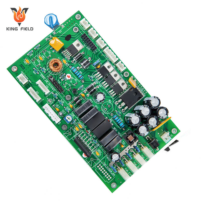
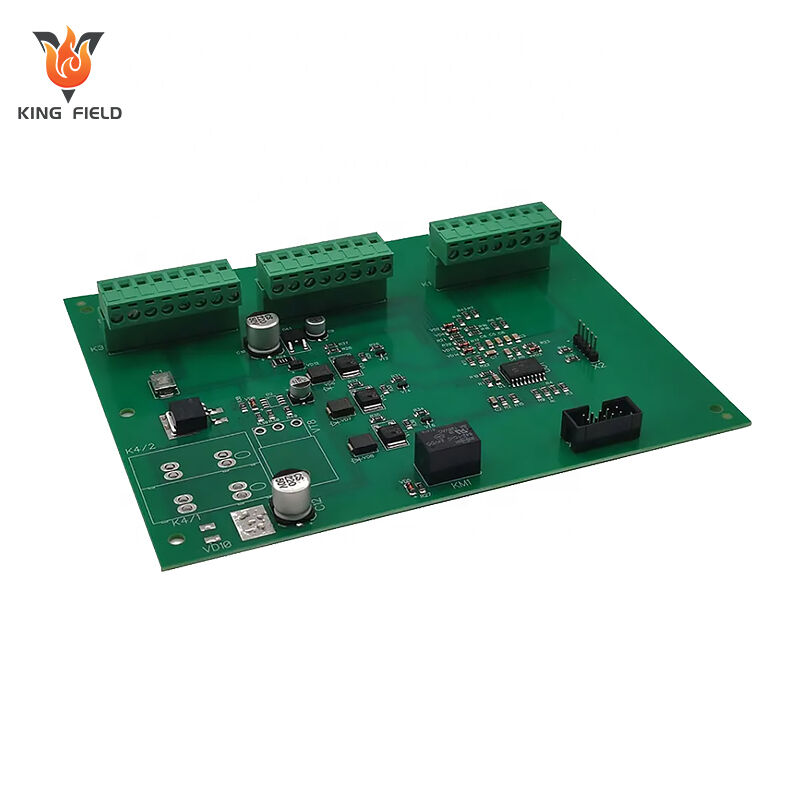
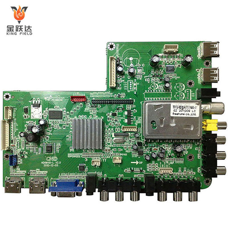
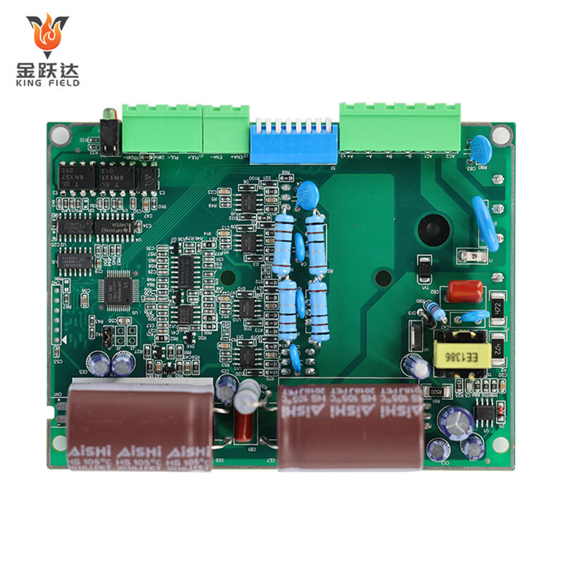
PCB design
PCB Design Overview
PCB design is the foundational process of creating a blueprint for electronic circuits—translating schematic diagrams into physical layouts that enable component mounting, electrical connectivity, and optimal performance.
Core Purpose of PCB Design
Convert electrical schematics into a manufacturable physical layout.
Ensure signal integrity, power distribution, and thermal management for reliable device operation.
Optimize size, weight, and cost while meeting technical requirements.
Common PCB Design Types
| Design Type | Description | Applications | |||
| Rigid PCB Design | Fixed, FR-4 based layouts | Consumer electronics, industrial controls | |||
| Flexible PCB Design | Bendable PI/PET substrates | Wearables, automotive dashboards | |||
| Rigid-Flex PCB Design | Combined rigid and flexible sections | Aerospace avionics, compact IoT devices | |||
| High-Frequency PCB | Optimized for signal integrity | Communication equipment, radar systems | |||
| Miniaturized PCB | Dense layouts with micro-components | Wearables, medical devices | |||
Critical Design Considerations
·Trace Width/Spacing: Follow IPC standards to ensure fabrication feasibility.
·Component Clearance: Avoid overcrowding for soldering access and heat dissipation.
·Thermal Management: Place high-power components with adequate spacing or heat sinks.
·Test Points: Add test pads for post-assembly inspection.
·Bend Radius: For flexible PCBs, maintain minimum bend radius to prevent trace damage.
Kingfield’s PCB Design Support
·DFM Review: Free pre-production design checks to identify manufacturability issues.
·Custom Design Services: End-to-end design for R&D prototypes or high-volume production.
·Compatibility Assurance: Align design with our assembly capabilities.
·Fast Iteration: Support design modifications for prototypes to accelerate time-to-market.
Whether you need to optimize an existing design or create a new PCB from scratch, Kingfield’s technical expertise ensures your design is manufacturable, reliable, and cost-effective. Contact our team to discuss your project requirements!
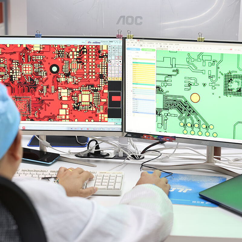
PCB Design Process
PCB Design Flow
1. Pre-Design Preparation
· Define Requirements: Clarify technical specs, form factor (size/weight), environment (temperature, vibration), and manufacturing constraints.
· Schematic Capture: Use EDA tools to draw component connections; include part numbers, values, and footprints.
· Component Sourcing & Verification: Confirm component availability and validate footprints to avoid assembly issues.
· Electrical Rule Check: Fix short circuits, incompatible components, or missing connections before layout.
2. PCB Layout Design
2.1 Setup Design Parameters
Define PCB size, shape, and layer stackup.
Set manufacturing rules: Trace width/spacing, hole sizes, pad clearances.
2.2 Component Placement
Place critical components first for optimal signal flow.
Follow DFM principles: Avoid overcrowding, ensure soldering access, and separate high-power/heat-generating components.
2.3 Trace Routing
Route signal traces: Optimize length and width.
Prioritize differential pairs and high-frequency traces for signal integrity; add ground planes to reduce noise.
Avoid sharp angles and crossing traces.
2.4 Design Rule Check
Run DRC to validate against layout rules.
Fix errors to ensure manufacturability.

3. Post-Layout Optimization & Verification
·Thermal Analysis: Simulate heat distribution and adjust component placement/heat sinks for high-power designs.
·Signal Integrity (SI) Simulation: Test high-frequency signals for reflection, crosstalk, or delay.
·DFM Review: Collaborate with Kingfield’s engineers to identify issues and optimize for assembly.
·Silkscreen & Solder Mask Setup: Add component labels, logos, and test points; define solder mask openings.
4. File Output & Handover to Manufacturing
·Generate Production Files: Export Gerber files, BOM (Bill of Materials), and pick-and-place files (for assembly).
·File Verification: Kingfield’s team reviews files to ensure compatibility with our fabrication/assembly processes.
·Prototype Order: Submit files for prototype production (3–7 business days) to test form, fit, and function.
5. Prototype Testing & Iteration
·Functional Testing: Validate the prototype’s electrical performance.
·Design Iteration: Adjust layout based on test results.
·Final Design Lock: Approve the optimized design for mass production.
Kingfield’s Support Throughout the Flow
·Pre-Design: Free requirement analysis and component sourcing support.
·Layout Phase: DFM reviews and custom stackup design for high-frequency/flexible PCBs.
·File Handover: Dedicated engineers verify production files and resolve compatibility issues.
·Prototyping: Fast prototype lead times + testing support to accelerate iteration.
Our PCB Design Services
1. Custom PCB Design
Schematic Capture: Convert your electrical concepts into EDA-ready schematics.
Component Selection & Sourcing: Access our global supplier network for verified, traceable components.
Layout Design: Optimized for signal integrity, thermal management, and space efficiency.
Layer Stackup Engineering: Tailored stackups for multi-layer PCBs and high-frequency applications.
2. Specialized Design Solutions
| Design Type | Key Applications | Technical Highlights | |||
| Rigid PCB Design | Consumer electronics, industrial controls, medical devices | FR-4/low-loss materials, dense component placement (01005 size support) | |||
| Flexible PCB Design | Wearables, automotive dashboards, IoT sensors | PI/PET substrates, 3D routing, minimum bend radius optimization | |||
| Rigid-Flex PCB Design | Aerospace avionics, compact IoT modules | Hybrid rigid-flex integration, weight reduction | |||
| High-Frequency PCB Design | 5G equipment, RF modules, radar systems | Controlled impedance, crosstalk minimization | |||
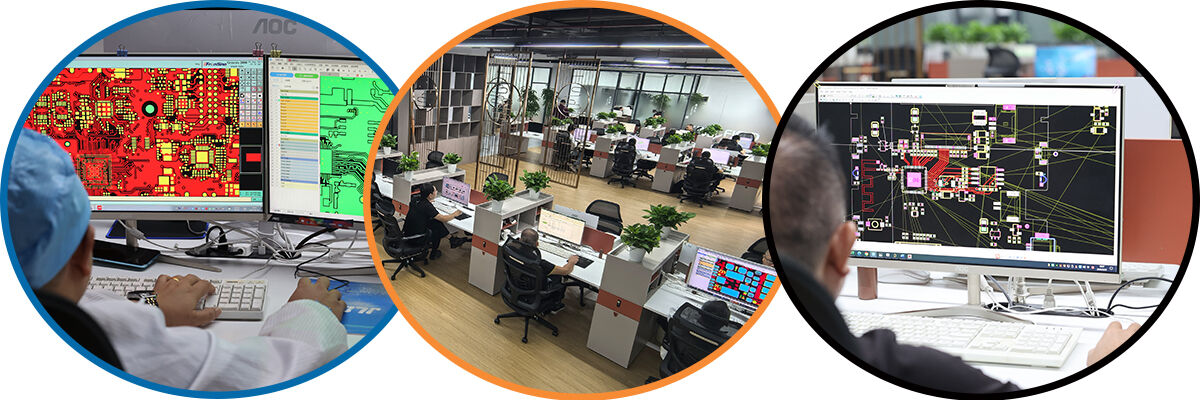
3. Design Verification & Optimization
Electrical Rule Check: Eliminate short circuits, incompatible components, and connection errors.
Design Rule Check: Validate against manufacturing constraints.
Signal Integrity Simulation: Test high-frequency signals for reflection, delay, and crosstalk.
Thermal Analysis: Optimize heat distribution for high-power components.
4. DFM Review & File Preparation
Free pre-production DFM reviews to identify manufacturability issues upfront.
Generate production-ready files: Gerber, BOM, pick-and-place, and assembly drawings.
File verification to ensure compatibility with Kingfield’s fabrication/assembly processes.
Why Choose Kingfield for PCB Design?
At Kingfield, we blend industry expertise, IPC compliance, and manufacturing-centric design to deliver PCBs that balance performance, cost, and scalability. Our end-to-end design services cater to prototypes, high-volume production, and specialized applications—backed by 20+ years of experience in rigid, flexible, and rigid-flex PCB design.
| Core Advantage | Details | ||||
| DFM-First Approach | Design optimized for manufacturability from day one, reducing rework and production delays. | ||||
| IPC-Certified Standards | Adheres to IPC-2221/2222/2223 standards for reliable, industry-compliant designs. | ||||
| Multi-Technology Expertise | Specializes in rigid, flexible, rigid-flex, high-frequency (5G/RF), and miniaturized PCBs. | ||||
| Fast Iteration Cycles | 3–7 day prototype turnaround + real-time engineering support to accelerate time-to-market. | ||||
| Full Turnkey Integration | Seamlessly connects design with our in-house PCB fabrication and assembly services. | ||||

