Quick Links
A Comprehensive Guide to PCB, PCBA, Assembly Methods, and Electronics Manufacturing
Printed Circuit Boards (PCBs) and Printed Circuit Board Assemblies (PCBAs) are at the very core of all modern electronics. From the smartphone in your pocket to advanced medical devices and automotive controls, PCBs and PCBAs make electronic functionality possible. Understanding the meaning of PCBA—Printed Circuit Board Assembly—and how it differs from a bare PCB is essential for engineers, product designers, electronics manufacturers, and even tech enthusiasts who want to grasp the basics and innovations of electronics manufacturing.
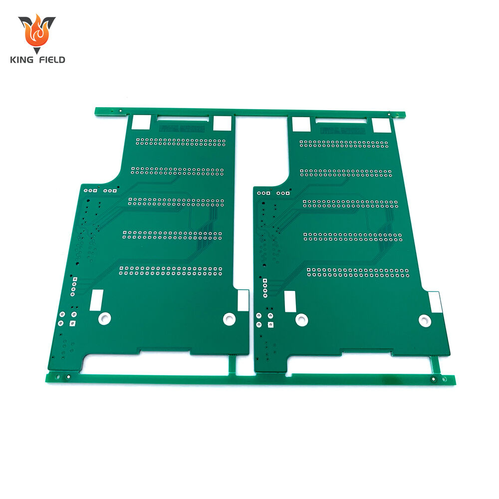
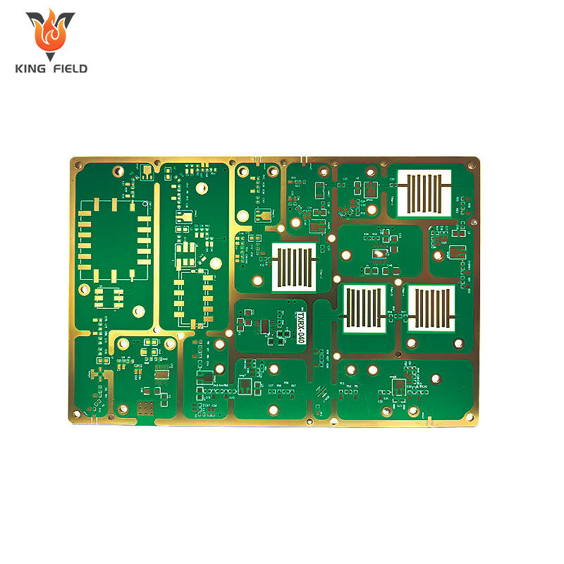
A PCB, or Printed Circuit Board, is a rigid board made of substrate material (often FR4), copper layers, and other materials. It serves as the backbone for mounting and electrically connecting electronic components such as resistors, capacitors, and integrated circuits (ICs). PCBs come in many forms, including single-sided, double-sided, and complex multilayered boards, supporting both simple gadgets and cutting-edge computing hardware.
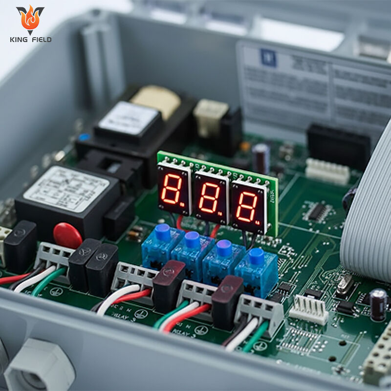
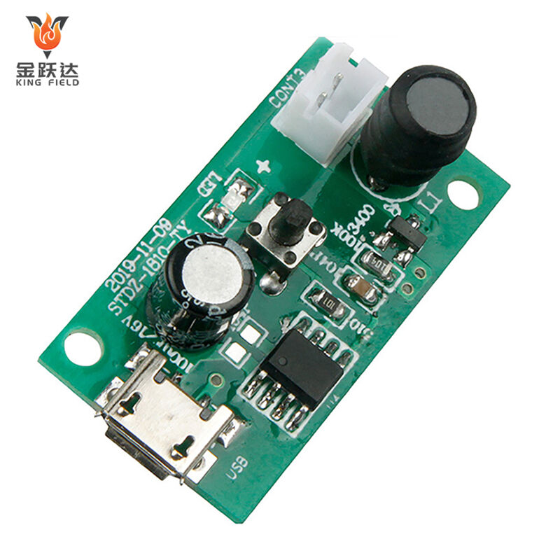
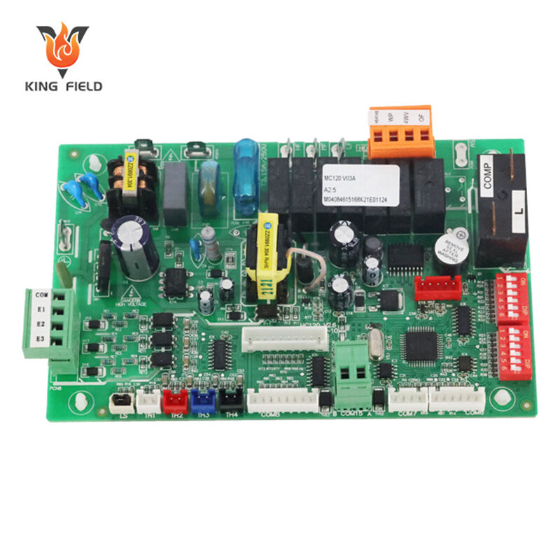
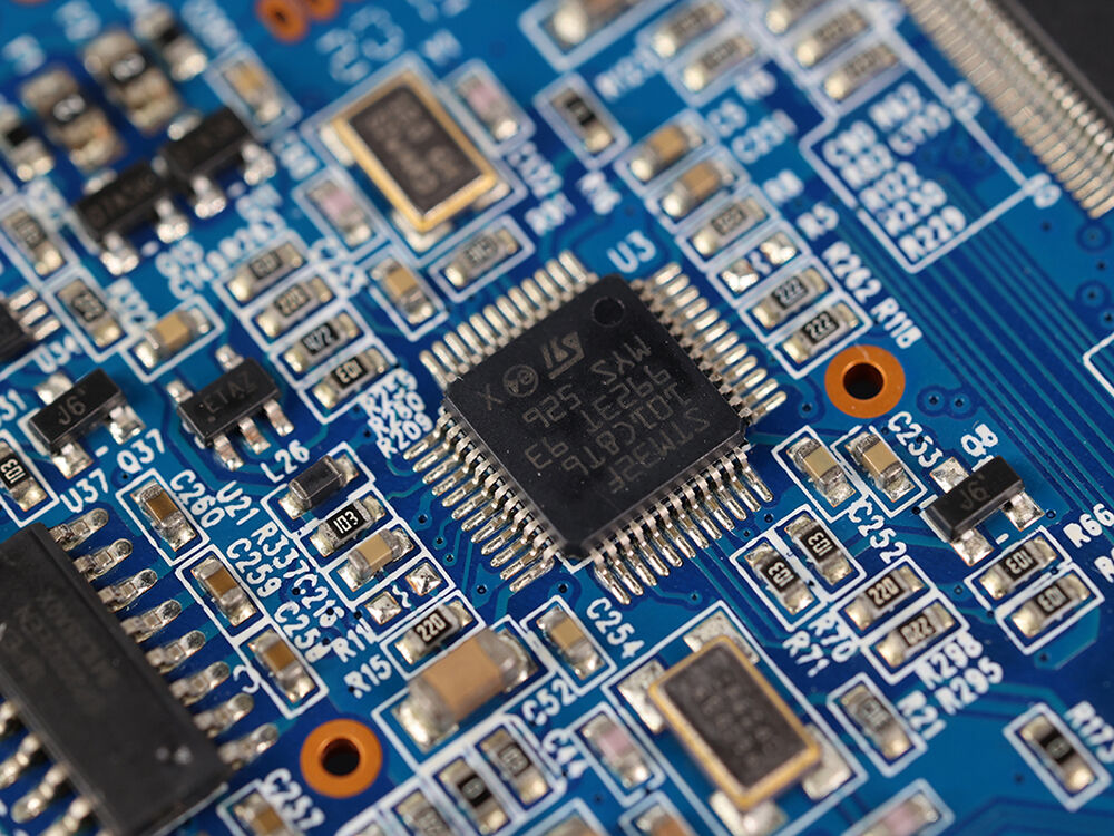
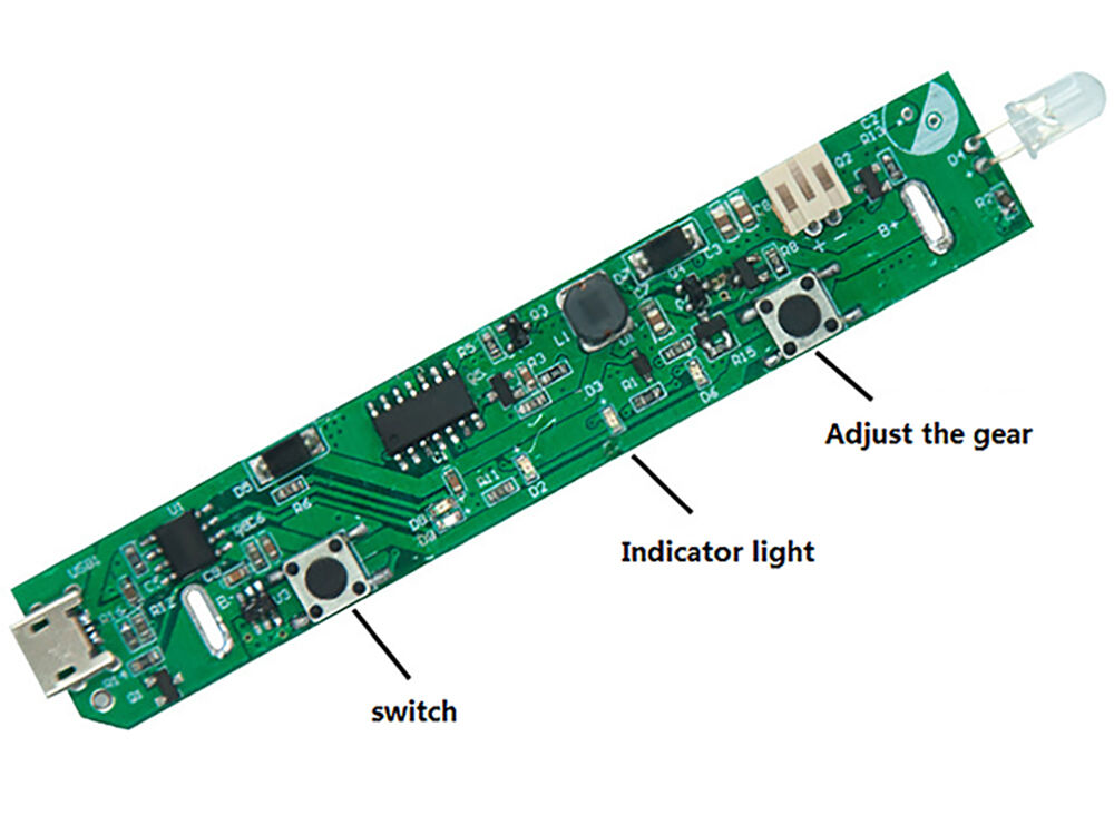
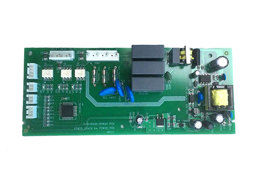
PCBA, or Printed Circuit Board Assembly, refers to the process and result of mounting and soldering electronic components onto a bare PCB—effectively transforming it from a passive platform to a fully functional, electronic device or module. This assembly process uses a variety of methods, including Surface-Mount Technology (SMT) and Through-Hole Technology (THT), and is backed by stringent quality control steps such as Automated Optical Inspection (AOI) and in-circuit testing.
Apply Solder Paste Solder paste is stenciled onto areas where components will be placed.
Placement of Components Automated pick-and-place machines position the components onto the board.
Soldering Most commonly done by reflow soldering (for surface-mount devices) or wave soldering (for through-hole components).
Inspection and Quality Control Visual inspection, Automated Optical Inspection (AOI), X-ray testing, and functional testing ensure quality.
Over 80% of all electronics use multilayer PCBs.
FR4 is the industry standard for most PCB fabrication due to its cost and balanced properties.
When discussing electronics manufacturing, it’s crucial to distinguish between a PCB (Printed Circuit Board) and a PCBA (Printed Circuit Board Assembly). While a PCB serves as a platform for electrical connectivity, a PCBA transforms this platform into a functional, ready-to-use electronic module through the process of mounting and soldering electronic components. Let’s dive deeper into the meaning, structure, and importance of PCBA in electronics production.
PCBA stands for Printed Circuit Board Assembly. It is the result of a meticulously managed process where all the necessary electronic components—such as resistors, capacitors, diodes, ICs, connectors, and more—are attached, soldered, and integrated onto a previously fabricated bare PCB. The resulting unit is a fully operational circuit board that can be directly integrated into consumer electronics, medical devices, automotive controls, or industrial machinery.
To put it simply, a PCB is the canvas, and PCBA is the finished painting. The assembly process adds functional value, enabling the board to perform its intended electrical tasks in a complete system.
A typical Printed Circuit Board Assembly consists of several vital elements:
Bare PCB: The foundation, fabricated as detailed in the previous section (usually FR4 substrate with copper traces, solder mask, and silkscreen).
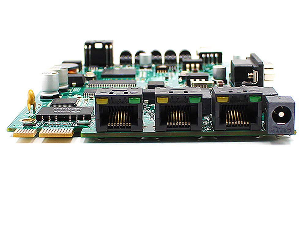
Electronic Components: Both passive components (resistors, capacitors, inductors) and active components (transistors, integrated circuits, diodes, microcontrollers, etc.) are attached.
Solder Paste: Applied to pads where components will be mounted; enables secure, conductive bonds through reflow soldering.
PCB Traces and Vias: Signal routes and interconnections remain essential in the assembled board.
PCB Cost: Generally lower since it involves only fabrication and materials (substrate, copper, solder mask). Cost is influenced by board size, the number of layers, trace width, via count, and yield.
PCBA Cost: Significantly higher due to:
Turning a PCB into a PCBA involves several key technologies and processes, each chosen based on end-use, component type, board complexity, and production volume:
Description: Electronic components are mounted directly onto the surface of the PCB using automated pick-and-place machines.
Process Steps:
Advantages: Speed, miniaturization, high assembly density—ideal for compact consumer devices, smartphones, wearables, and IoT boards.
Quality Control: Solder Paste Inspection (SPI) and Automated Optical Inspection (AOI) ensure placement accuracy and solder joint quality.
Often, a combination of SMT and THT is used for complex boards—for example, SMT for miniaturized logic and THT for large connectors or power electronics.
Quality control is non-negotiable in the PCB assembly process. After assembly, every PCBA undergoes rigorous validation, including:
In-Circuit Test (ICT): Verifies correct component placement, solder joints, and basic functionality.
Functional Circuit Test (FCT): Simulates real-world operation to ensure the circuit performs as intended.
Flying Probe Test: Flexible probe-based test for prototypes or low-volume runs.
X-ray Inspection: Used to inspect soldering quality for BGAs (Ball Grid Arrays) and hidden joints, especially crucial for high-reliability applications.
Aging Test and Harsh Environment Simulation: Simulates prolonged operational stress or harsh conditions (temperature, vibration) for automotive or industrial use.
Did You Know? Advanced PCBA testing protocols have contributed to increasing the reliability of automotive and medical electronics, drastically reducing field failures and warranty returns.
Rapid Prototyping: Quick-turn PCBA accelerates the journey from schematic design to functional prototype—vital for startups and R&D teams.
Consistency and Scale: Automated assembly yields high repeatability, tight tolerances, and low unit-to-unit variation—key for quality and regulatory compliance.
Cost Efficiency: While PCBA assembly adds cost over a bare PCB, it saves time, labor, and reduces errors compared to manual point-to-point wiring.
Flexibility: Modern PCBA lines handle from single prototypes to mass production for products in consumer electronics, automotive, defense, and IoT.
|
PCB vs PCBA |
PCB (Printed Circuit Board) |
PCBA (Printed Circuit Board Assembly) |
|
State |
Bare, without attached electronic components |
Fully assembled with all required electronic components |
|
Function |
Provides structure and circuit pattern |
Operates as a functional device or module |
|
Manufacturing |
Involves layout, fabrication, drilling, plating, masking |
Adds pick-and-place, soldering, quality control, and device programming |
|
Applications |
Used for prototyping, custom board development |
Used in finished products—consumer, automotive, medical, industrial, and more |
|
Cost |
Lower initial cost |
Higher assembly cost, but needed for functionality |
|
Testing |
Basic electrical tests (opens/shorts) |
Includes functional, in-circuit, and advanced inspections |
Understanding the nuanced differences between PCB (Printed Circuit Board) and PCBA (Printed Circuit Board Assembly) is fundamental for making informed choices in electronics development, prototyping, or mass manufacturing. While both terms are interconnected, they represent distinctly different stages in the journey from design to a working electronic device. Below, we’ll explore these distinctions in-depth, considering state, functionality, manufacturing steps, testing requirements, costs, and real-world applications.
PCB (Printed Circuit Board): PCBs start as blank, layered substrates with patterned copper traces. At this stage, the board does not perform any electrical function other than enabling connectivity once components are attached. A PCB is passive and non-functional on its own.
PCBA (Printed Circuit Board Assembly): Once electronic components are mounted, soldered, and tested, the board becomes a PCBA. PCBA functionalities vary widely, from power management circuits in IoT devices to advanced computational modules in artificial intelligence hardware. It is the “activated” form, ready to perform complex operations in real-world devices.
|
Parameter |
PCB |
PCBA |
|
Initial Tests |
Opens/shorts on copper traces |
ICT, FCT, AOI, X-ray, flying probe |
|
Defect Types |
Shorts, opens, missing vias |
Placement errors, solder joint defects, faulty or incorrect components |
|
Post-Production |
Visual and electrical testing |
Stress testing, aging, full system verification |
|
Tools Used |
Flying probe, continuity tester |
AOI, X-ray, dedicated functional testers, and simulation systems |
|
Scenario |
Best Choice |
Reason |
|
Prototype electrical circuit |
PCB |
Rapid iteration, easy manual assembly |
|
Functional testing/field demo |
PCBA |
Fully operational, ready for software & system integration |
|
Low cost, design validation |
PCB |
Affordable for multiple concept revisions |
|
High-volume manufacturing |
PCBA |
Assemblies delivered ready for immediate integration, cost-effective at scale |
|
Feature |
PCB (Printed Circuit Board) |
PCBA (Printed Circuit Board Assembly) |
|
Form |
Bare board, no components |
Assembled, with all required components |
|
Functionality |
Non-functional; substrate only |
Operational electronics; ready for system integration |
|
Manufacturing |
Board fabrication only |
Board fabrication + complex assembly + advanced testing |
|
Cost |
Lower |
Higher (components, labor, testing) |
|
Applications |
Prototyping, R&D, education |
Consumer, industrial, automotive, aerospace, medical |
|
Testing |
Basic electrical continuity |
In-circuit, functional, automatic and manual inspectio |
A Printed Circuit Board (PCB) is the foundational building block of nearly every electronic device. At its core, a PCB is a thin board made from insulating material, most commonly FR4 (a fiberglass-reinforced epoxy laminate), with one or more layers of conductive copper traces. These traces act as the "wiring" that connects and routes electrical signals between different electronic components—including passive components (like resistors and capacitors) and active components (such as transistors and integrated circuits).
A well-designed PCB is more than just a replacement for traditional wiring. It ensures signal integrity, mechanical support, electrical insulation, and heat dissipation, all of which are critical for long-term PCB reliability and performance. The mechanical layout of the PCB not only supports component placement but also dictates electrical properties such as trace impedance, PCB layer structure, and signal isolation.
Modern circuits demand varying PCB stackup and designs depending on complexity, operating frequency, and environment.
|
Type of PCB |
Description |
Typical Application |
|
Single-Sided PCB |
One copper layer, simplest to manufacture, low cost. |
Simple toys, calculators, radios |
|
Double-Sided PCB |
Copper layers on both sides, allows more complex circuits and signal routing. |
Power supplies, automotive systems |
|
Multilayer PCB |
Three or more copper layers, separated by insulating substrate. Allows for compact, powerful boards with extensive interconnects. |
Computers, telecom, medical devices |
Substrate (Dielectric Layer): Provides structural integrity and insulation. Most common is FR4, known for its balance of strength, cost, and electrical performance.
Copper Layers: Thin layers of copper foil etched into conductive traces. The number of copper layers defines the board's capability—multilayer PCBs are standard in high-performance electronics.
Solder Mask: The green (or sometimes red, blue, or black) resin coating that insulates copper traces and prevents solder bridges during component soldering.
Silkscreen: White printed labels for parts and reference designators, crucial for component placement accuracy during PCB assembly.
Vias: Small plated holes that electrically connect copper layers—essential for routing signals in complex multilayer boards.
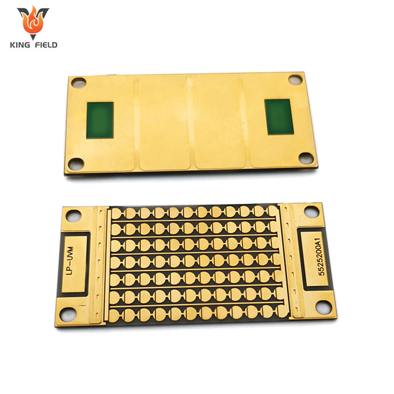
Edge Connectors (Gold Fingers): Gold-plated contacts used for board-to-board or board-to-edge device connections, vital in expansion cards and memory modules.
At KINGFIELD, we provide comprehensive PCBA services to meet the needs of innovators, engineers, and manufacturers across a range of industries. Our solutions ensure high-quality, reliable, and efficient printed circuit board assembly for every project.
Prototype PCBA: Rapid prototyping and quick-turn assemblies to help you test and refine new designs fast.
Turnkey PCBA Manufacturing: Complete, end-to-end assembly service—from purchasing components, PCB fabrication, assembly, testing, and delivery.
Surface Mount Technology (SMT) Assembly: High-speed, automated SMT assembly for small, complex, or high-volume projects.
Through-Hole Assembly: Manual or automated through-hole assembly for components that require strong mechanical bonds.
Mixed-Technology Assembly: Seamless integration of SMT and through-hole components in a single assembly.
Component Sourcing & BOM Management: Professional sourcing to ensure component quality, availability, and cost-effectiveness.
Functional Testing & Inspection: In-circuit testing, Automated Optical Inspection (AOI), X-ray, and functional testing to guarantee quality and performance.
Box Build & Final Product Assembly: Complete enclosure assembly, wiring, and sub-assembly solutions to deliver a finished ready-to-use electronic product.
Whether you need prototypes, small batches, or mass production, our PCBA services are designed to ensure your products are built to perform—on time and on budget.
 Hot News
2026-01-17
2026-01-16
2026-01-15
2026-01-14
2026-01-13
2026-01-12
2026-01-09
2026-01-08