Rigid Flex PCB
High-performance Rigid-Flex PCBs for medical, industrial, automotive & consumer electronics. Seamless integration of rigid stability and flexible adaptability—ideal for space-constrained, complex devices. Precision fabrication, enhanced signal integrity, 24h prototyping, fast delivery, DFM support & AOI testing ensure reliable performance in demanding applications.
✅ Rigid-flex hybrid design
✅ 24h prototyping | fast turnaround
✅ DFM optimization & quality testing
✅ Multi-industry compact device compatibility
Description
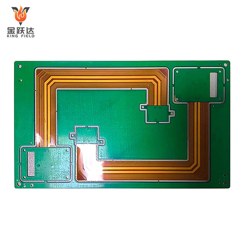
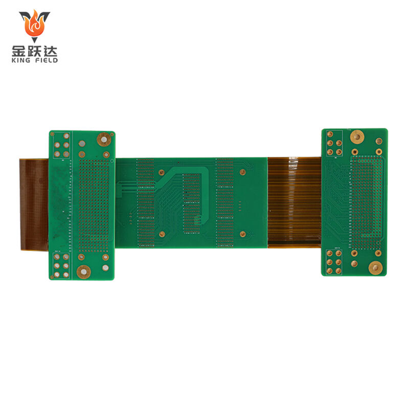
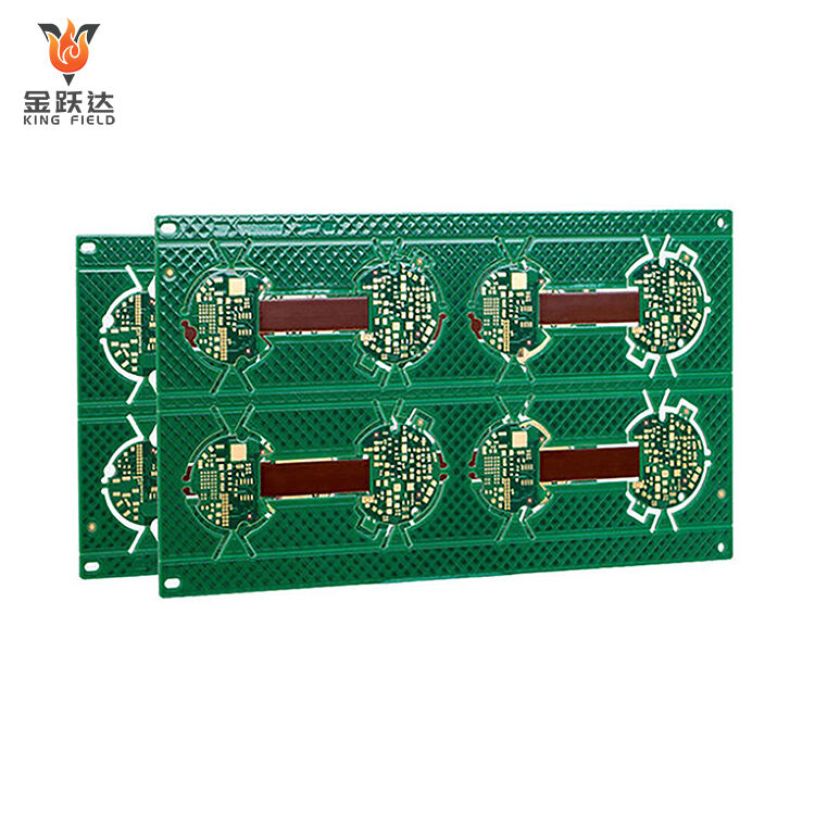
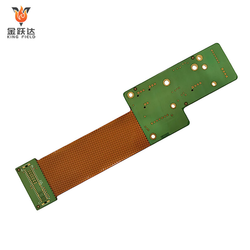
Rigid-flex PCB
Rigid-flex PCB combines the advantages of flexible circuits and traditional Rigid circuit boards. Its physical structure is: flexible circuit layers are sandwiched between rigid circuit layers. The rigid and flexible circuit boards are partially bonded together by prepregs, which are glass fiber reinforced dielectric materials that are cured by heating and pressure. This structure combines the advantages of a flexible and lightweight circuit with a rigid layer that has strong mechanical stability.
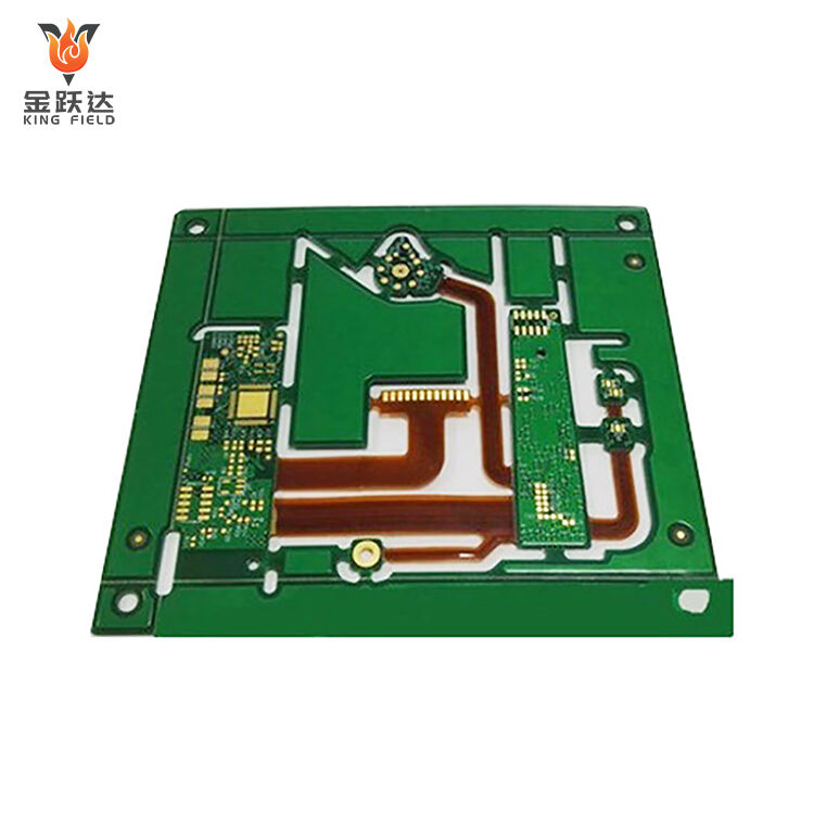
A key component of rigid-flex composite panels
· Rigid cross-section:
Provide mechanical stability and structural support
Use traditional materials such as FR-4 or special laminates
Supports surface mount components and connectors
Provide standard mounting surfaces for assembly
· Flexible part:
Made of polyimide or polyester substrate
Achieve bending, folding and dynamic movement
Rigid components can be connected without cables or connectors
Allow three-dimensional configuration
· Transition Zone:
The key area where the rigid part and the flexible part converge
Careful design is needed to prevent mechanical stress
Use specialized materials and construction techniques
Determine the overall reliability of the circuit board
| Feature | Description | ||||
| Structure | Rigid layers (FR-4, etc.) + Flexible layers (Polyimide, etc.) + Adhesive layers + Conductive layers | ||||
| Key Advantages |
1. Reduce connectors/cables, lower failure risk; 2. Save space for complex assemblies; 3. Enhance product reliability and durability; 4. Simplify assembly process, cut costs |
||||
| Limitations | High design complexity; Higher manufacturing cost than traditional PCB; Long modification cycle |
Application Scenarios
Consumer Electronics: Smartphones, laptops, wearables
Automotive Electronics: On-board radar, instrument panels, BMS for new energy vehicles
Industrial Equipment: Robot joints, sensor modules, medical devices
Aerospace: Satellite equipment, UAV control systems
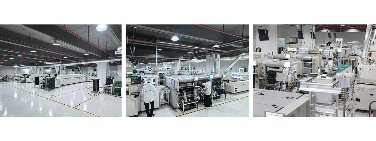
Production Capacity
| Items | Rigid-flex | ||||
| Material | FR-4,FPC High-frequency | ||||
| Layers | 1-40L | ||||
| Max cut lamination size | 500*420mm | ||||
| Final board thickness | 0.20-6.0mm | ||||
| Min Final Hole size | 0.075mm | ||||
| Aspect Ratio | 0.584027778 | ||||
| Inner layer Line Width/Space | 0.05mm | ||||
| Copper Foil Thickness (Inner Layers) | 1/6oz-1oz | ||||
| Min dielectric layer thickness | 20um | ||||
| Copper Foil Thickness (Outer Layers) | 1/3oz-1oz | ||||
| Copper to drill distance | 0.2mm | ||||
| Out layer Line width/space | 0.035mm | ||||
| Min SMD width | 0.05mm | ||||
| Max Solder Mask Plug Hole Diameter | 0.5mm | ||||
| solder mask strip width | 0.075mm | ||||
| Final Set Size Tolerance | ±0.1mm/limit±0.05mm | ||||
| Min Hole to board edge Distance | 0.075-0.15mm | ||||
| Min Beveling angle Tolerance | ±3-5° | ||||
| Layer to layer Tolerance | ≤0.075mm(1-6L) | ||||
| Inner layer Min PTH Annular Ring | 0.15mm | ||||
| Out layer Min PTH Annular ring | 0.15mm | ||||
| Surface Treatment | OSP、HASL 、ENIG、Gold Finger、Plating Gold 、ENEPIG、IMM TIN、IMM AG | ||||
| Warp&Twist | 0.5%(less than 45u) | ||||
Material selection
Flexible substrate: Polyimide has become the preferred choice due to its reliability and heat resistance.
Rigid core material: FR-4 is used for standard applications, and special laminates are used for high-performance requirements
Prepregs: Non-flowing or low-flowing prepregs can prevent resin from seeping into flexible areas.
Adhesive: An acrylic or epoxy resin system used for bonding the coating layer
Standard flexible material
Polyimide (Kapton) 0.5 mil to 5 mil (0.012mm - 0.127mm)
Copper-clad substrate without adhesive, with a thickness of 1 to 5 mils
Flame-retardant laminates, substrates and coverings
High-performance epoxy resin laminates and prepregs
High-performance polyimide laminates and prepregs
Materials that comply with UL and RoHS standards can be provided upon request
High Tg FR4 (Tg 170+), polyimide (Tg 260+)
| PCB Manufacturing Capability | |||||
| ltem | Production capability | Min space for S/M to pad, to SMT | 0.075mm/0.1mm | Homogeneity of Plating Cu | z90% |
| Layer Count | 1~40 | Min space for legend to pad/ to SMT | 0.2mm/0.2mm | Accuracy of pattern to pattern | ±3mil(±0.075mm) |
| Production size | 250mmx40mm/710mmx250mm | Surface treatment thickness for Ni/Au/Sn/OSP | 1~6um /0.05~0.76um /4~20um/ 1um | Accuracy of pattern to hole | ±4mil (±0.1mm ) |
| Copper thickness of lamination | 1/3 ~ 10z | Min size E- tested pad | 8 X 8mil | Min line width/space | 0.045 /0.045 |
| Product board thickness | 0.036~2.5mm | Min space between tested pads | 8mil | Etching tolerance | +20%0.02mm) |
| Auto-cutting accuracy | 0.1mm | Min dimention tolerance of outline | ±0.1mm | Cover layer alignment tolerance | ±6mil (±0.1 mm) |
| Drill size | 0.075mm/6.5mm/±0.025mm | Min dimention tolerance of outline | ±0.1mm | Excessive adhesive tolerancefor pressing C/L | 0.1mm |
| Warp&Twist | ≤0.5% | Min R corner radius of outline | 0.2mm | Alignment tolerance forthermosetting S/M and UV S/M | ±0.3mm |
| maximum aspect Ratio(thickness/hole diameter) | 8:1 | Min space golden finger to outline | 0.075mm | Min S/M bridge | 0.1mm |
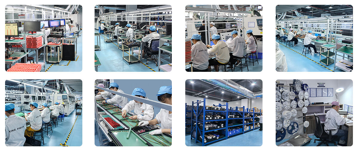
Why Choose Us
· Expert Rigid-Flex PCB Manufacturing
We specialize in producing high-quality rigid-flex PCBs, leveraging extensive experience and advanced equipment. Our rigid-flex PCBs are not only structurally reliable but also provide excellent electrical performance, making them ideal for compact and complex electronic devices requiring high stability and precision.
· Support for Complex Designs
We offer multilayer, high-density rigid-flex PCBs that meet the needs of complex circuit designs and stringent space constraints. Whether for industrial control systems, medical devices, or consumer electronics, our products cater to demands for miniaturization, high performance, and flexible connections, with exceptional design and engineering support.
· Flexible Customization
To meet the diverse needs of our clients, we provide flexible customization services. From material selection and thickness configuration to specialized functional designs, we tailor rigid-flex PCB solutions according to specific application requirements, ensuring optimal performance in various use cases.
· High Reliability and Durability
Every step of our rigid-flex PCB manufacturing process undergoes strict quality control to ensure high reliability and durability. Rigorously tested and inspected, our products perform consistently even under high stress and harsh environments, making them suitable for demanding industries such as aerospace, automotive electronics, and high-end consumer electronics.
Frequently Asked Questions
Q1.What files do you require for PCB manufacturing?
A:To start PCB manufacturing, we would require various design files including Gerber Files, Bill of Materials (BOM) file, Assembly drawings, Preliminary files or any other special requirements file.
Q2.How long is rigid flex PCB lead time, usually?
A:The lead time for such boards is 1 to 2 weeks; however, it will depend on the bespoke requirements.
Q3.What quality compliance are you providing for rigid-flex circuit boards?
We manufacture rigid flex circuit boards, rigid PCBs and flex PCBs in accordance with UL, ISO-9001, AS 9100, IPC-6012/6013 and MIL performance standards.
Q4.What surface finishes do you offer for rigid flex PCBs?
A:We offer Immersion Ni/Au and OSP. We also provide custom surface finishing or plating for rigid flex circuit boards.
Q5.What stiffener material do you use?
A:We use FR4, steel or aluminum.

