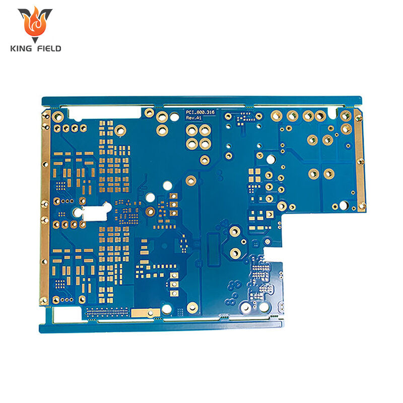
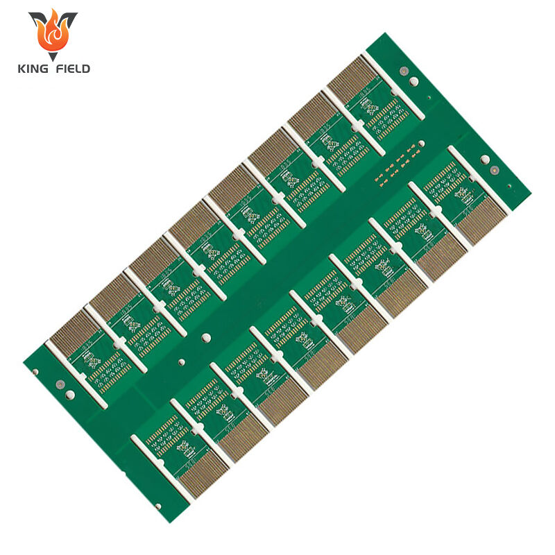
HDI PCB
High-Density Interconnect (HDI) PCBs for compact, high-performance electronics (medical/industrial/automotive/consumer). Fine-pitch traces, microvias, and space-saving designs—paired with 24h prototyping, fast delivery, DFM support & strict testing. Boost signal integrity, reduce size, and power your next-gen products.
Description
About HDI PCBs
High-density interconnect (HDI) PCBs achieve miniaturization and high performance of electronic devices through advanced through-hole technology.
What is an HDI PCB?
HDI PCB stands for High-Density Interconnect PCB. According to IPC-2226, HDI is defined as a printed circuit board with a higher wiring density per unit area than a conventional printed circuit board (PCB). It is manufactured using micro-blind via technology, resulting in high circuit density.
Features of HDI PCBs:
- Enhanced Signal Integrity:
HDI technology utilizes in-board vias, blind vias, and buried vias to bring components closer together, shortening signal path lengths and improving signal quality.
- Cost-Effectiveness:
With proper planning, HDI technology can reduce overall cost compared to standard PCBs. This is achieved through fewer layers, smaller dimensions, and a reduction in the number of PCBs required.
- Improved Reliability:
Compared to traditional vias, microvias have a smaller aspect ratio, providing higher reliability. They are also more robust.
- Compact Design:
The use of blind and buried vias minimizes board space requirements, making electronic devices smaller and lighter.
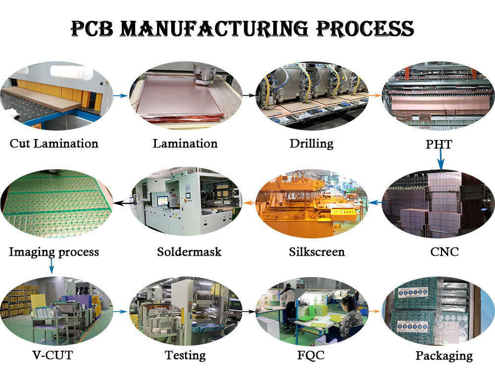
Manufacturing capacity
Manufacturing Capabilities
Kingfield offers advanced HDI PCB manufacturing technology and rigorous quality control.
| Feature | Capability | ||||
| Via Types | Blind via, buried via, through-hole via | ||||
| Number of layers | Up to 60 layers (evaluation required above 30 layers) | ||||
| HDI builds | 1+N+1, 2+N+2, ..., 6+N+6(≥6 orders require evaluation) | ||||
| Copper weights (finished) | 18um-70um | ||||
| Min trace/spacing | 0.065mm/0.065mm | ||||
| PCB thickness | 0.1-8.0mm (evaluation required for less than 0.2mm or greater than 6.5mm) | ||||
| Max. PCB dimension (finished) | 2-20 layers, 21×33 inches; length ≤ 1000mm; evaluate if short side > 21 inches | ||||
| Min. mechanical drilling | 0.15mm | ||||
| Min. laser drilling | Standard 4 mil, 3 mil require evaluation (corresponding to single 106PP) | ||||
| Max. laser drilling | mil (corresponding dielectric thickness cannot exceed 0.15mm) | ||||
| Min. controlled depth drilling | PTH: 0.15mm; NPTH: 0.25mm | ||||
| Aspect ratio | Max 14:1; evaluate if greater | ||||
| Min. solder mask bridge | 4mil (green, ≤1OZ) 5mil (other colors, ≤1OZ) | ||||
| Diameter range of resin-filled vias | 0.254-6.5mm | ||||
Type
HDI PCB Stacking
Kingfield offers a variety of HDI stacking configurations to meet your specific design requirements.
| Common stacking configurations | Layer overlay design | ||||
| 1 + N + 1 layered spiral flight | Understanding different HDI PCB stack-up structures helps designers gain greater flexibility in layer assignment, component placement, and routing options, thereby effectively utilizing available space and optimizing PCB layout. The left figure shows a common HDI PCB stack-up structure. | ||||
| Top solder mask | |||||
| Top grade copper (1 oz) | |||||
| Prepreg (0.06 mm) | |||||
| Core (N layers) | |||||
| Prepreg (0.06 mm) | |||||
| Bottom copper (1 oz) | |||||
| Bottom solder mask | |||||
|
Application areas: consumer electronics, mobile devices, IoT sensors |
|||||
|
Advantages: High cost-performance ratio, good balance between density and performance. |
|||||
| 2 + N + 2 layered hovering flight | |||||
| Top solder mask | |||||
| Top grade copper (1 oz) | |||||
| Prepreg (0.06 mm) | |||||
| Copper inner lining (1 oz) | |||||
| Prepreg (0.06 mm) | |||||
| Core (N layers) | |||||
| Prepreg (0.06 mm) | |||||
| Copper inner lining (1 oz) | |||||
| Prepreg (0.06 mm) | |||||
| Bottom copper (1 oz) | |||||
| Bottom solder mask | |||||
|
Application areas: High-performance computing, automotive electronics, medical devices |
|||||
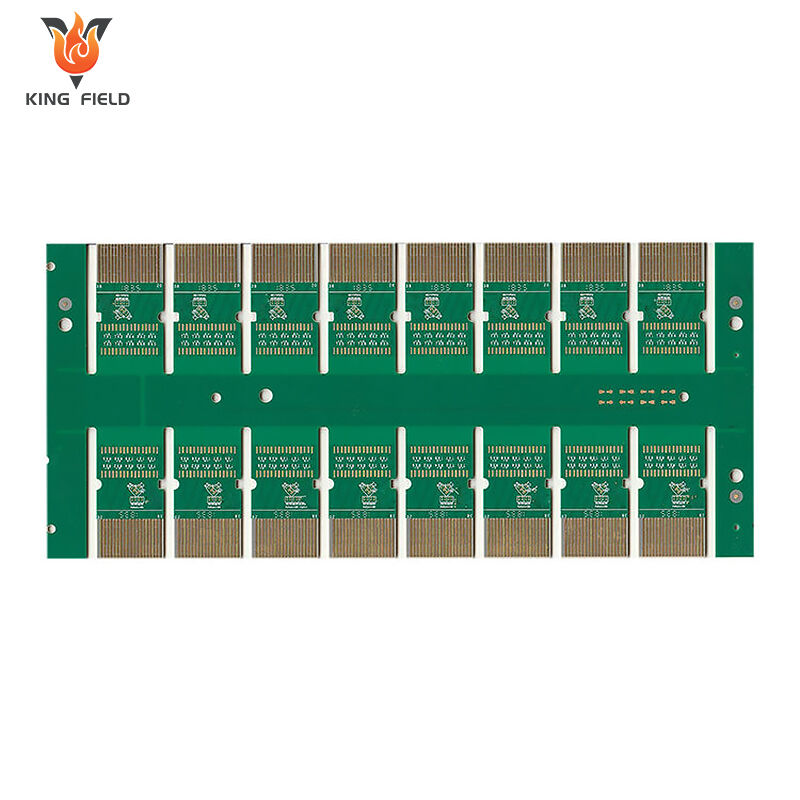
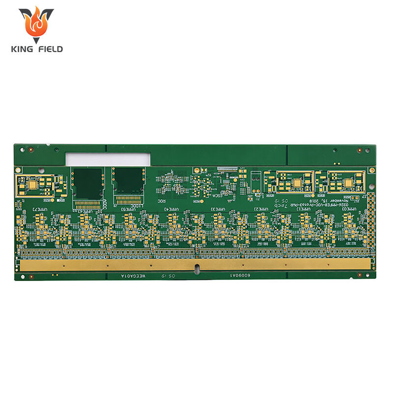
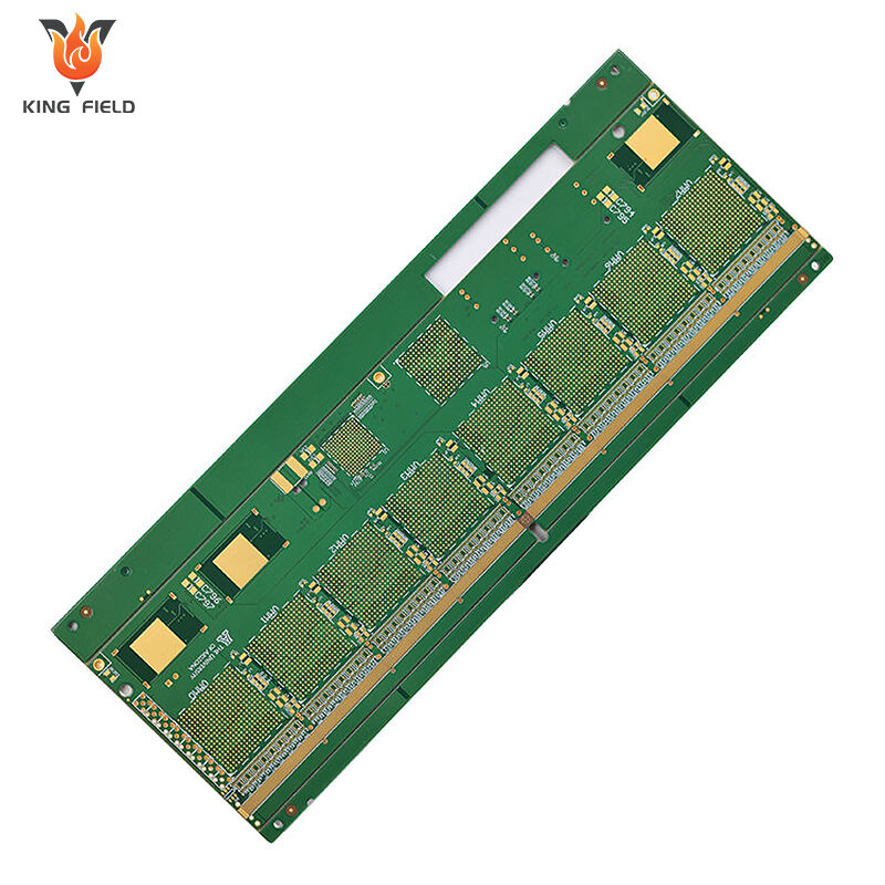
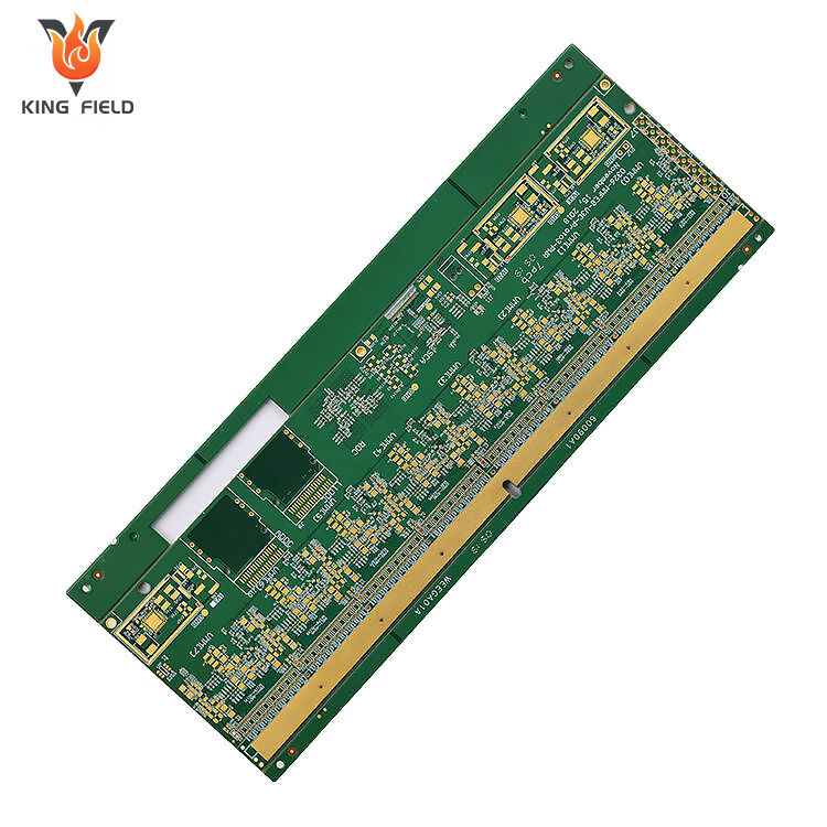
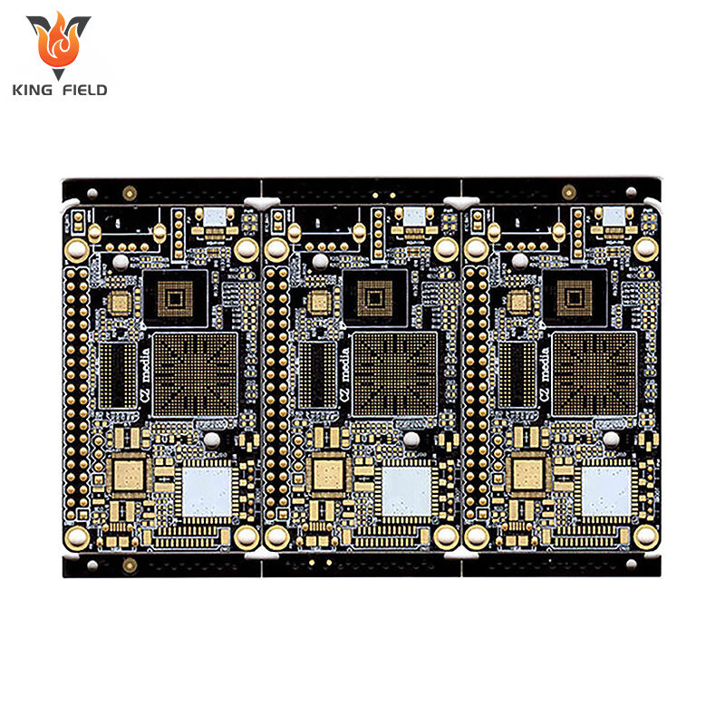
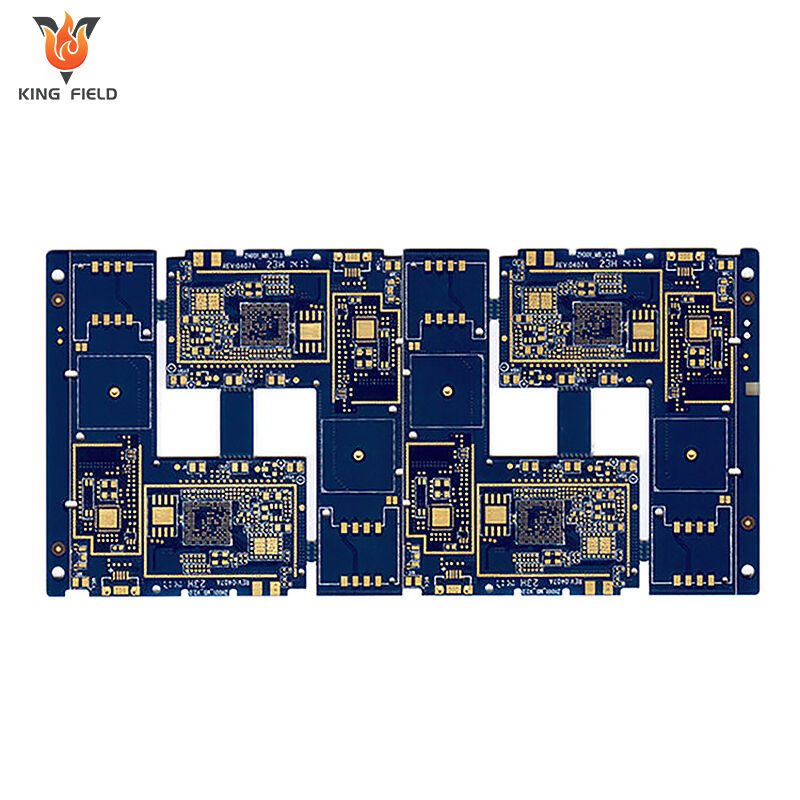
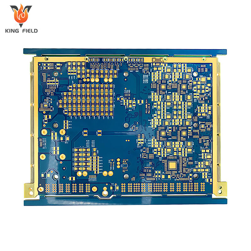
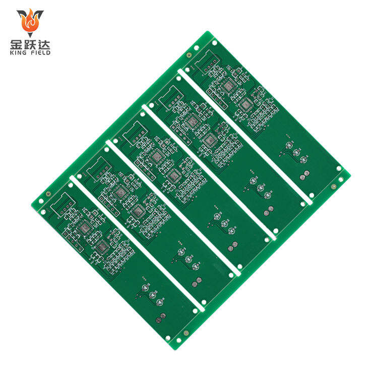
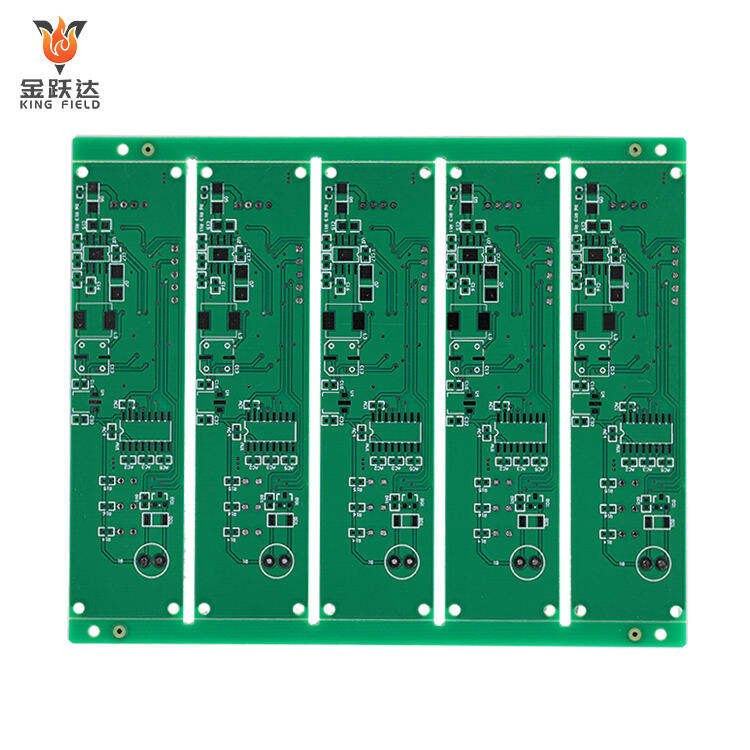
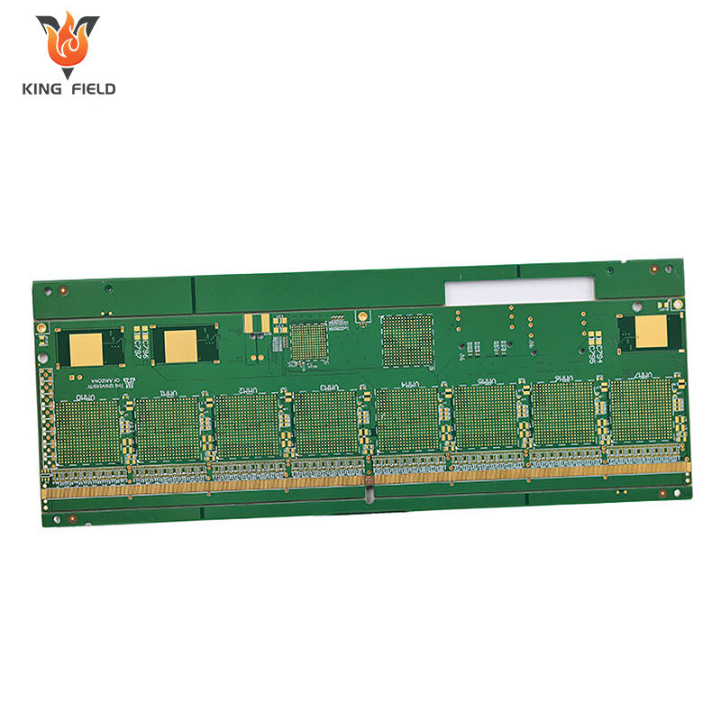
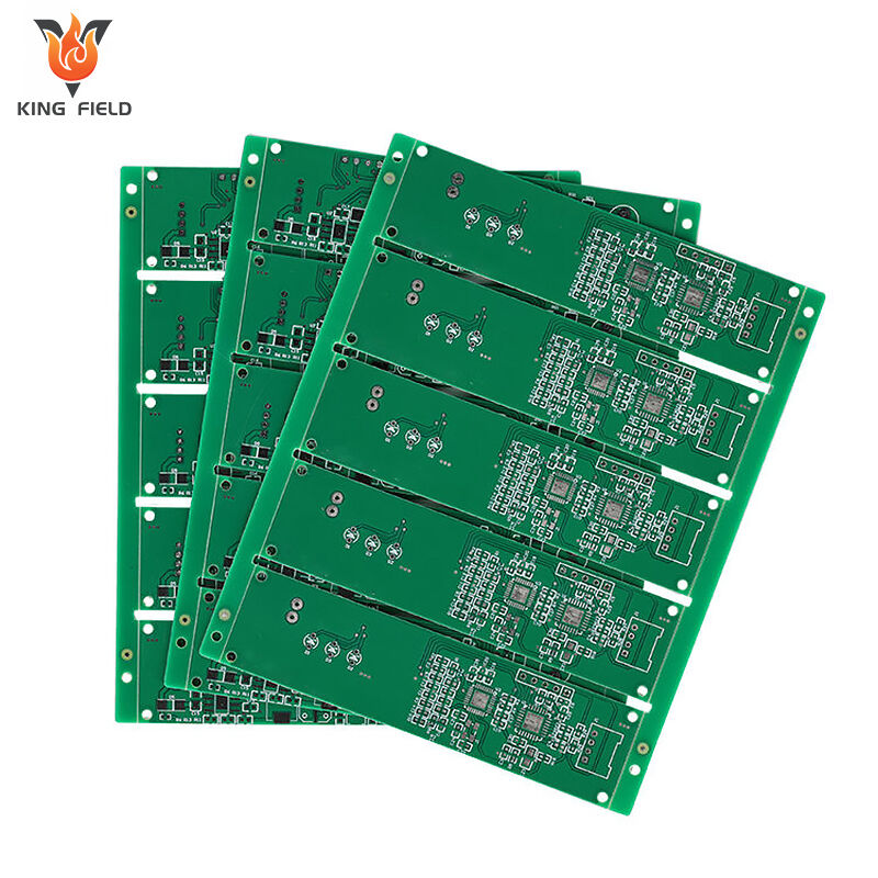
Case
Case Studies
Exploring Our Successful HDI PCB Projects Across Different Industries
 |
 |
 |
|
Consumer Electronics Products
|
Medical Devices
|
Automotive
|

