Quick Links
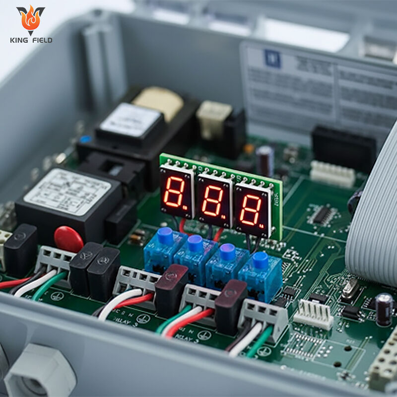
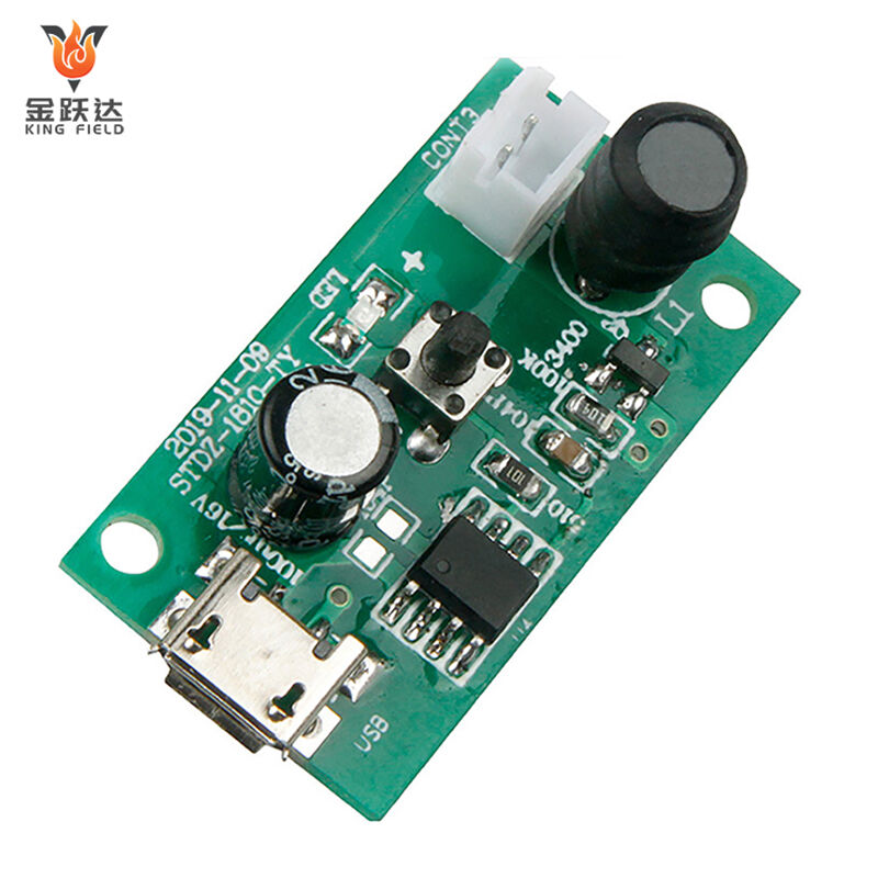
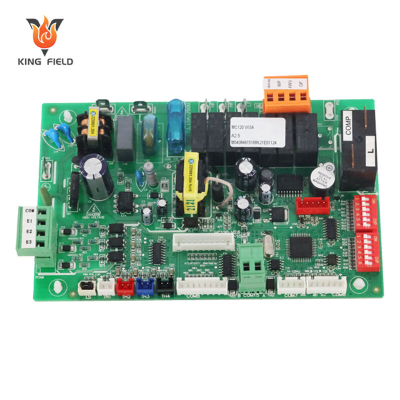
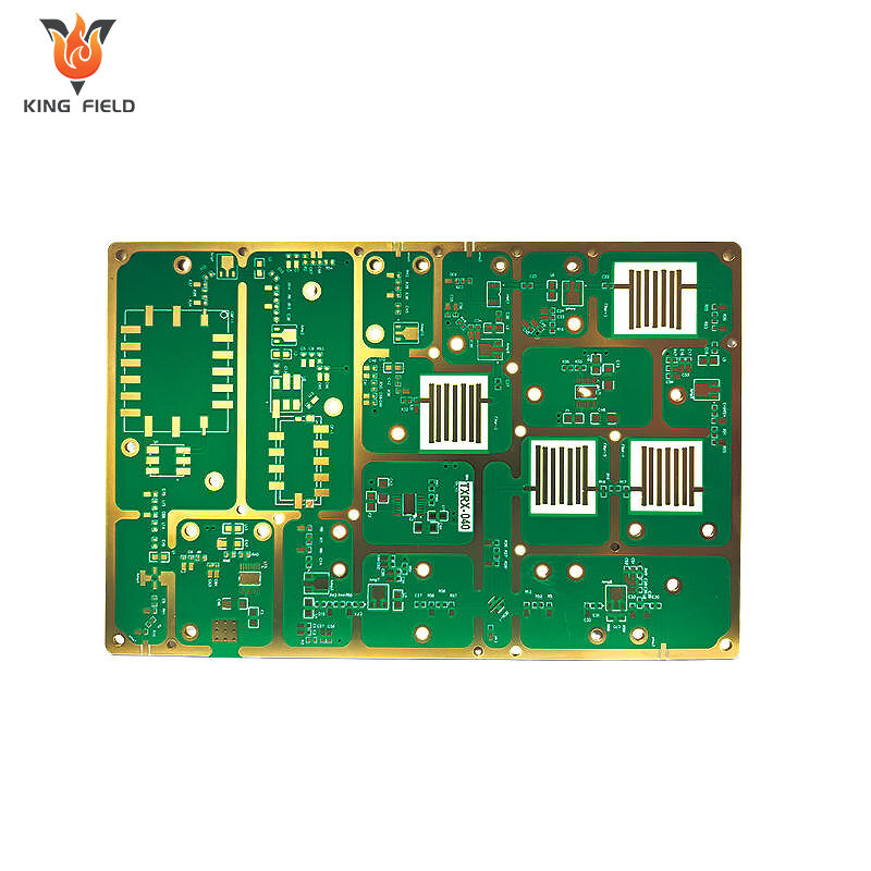
Surface Mount Technology (SMT) is a foundational process used in modern PCB assembly for attaching electronic components directly onto the surface of printed circuit boards (PCB). These components, known as Surface Mount Devices (SMDs), differ from those used in the older Through-Hole Technology (THT) method, where parts are inserted into drilled holes and soldered on the opposing side. SMT forgoes these drilled holes, instead leveraging tiny pads and highly precise soldering techniques to mount components, enabling a significant leap in manufacturing efficiency, miniaturization, and circuit complexity.
The primary shift with SMT was the move from manual, labor-intensive assembly to automation-driven production. With THT, assembly lines required significant manual labor, specialized component leads, and multiple soldering steps per part—making high-density boards costly and time-consuming to fabricate. SMT, by contrast, utilizes pick-and-place machines and reflow ovens, which streamline the assembly process, minimize assembly expenses, reduce human error, and unlock the potential for high-volume production without sacrificing quality or signal performance.
Key facts about SMT:
SMT is not simply an evolution of THT; it represents a paradigm shift in how boards are designed, manufactured, and assembled. To clarify the differences, here’s a comparative snapshot:
|
Technology |
SMT (Surface Mount) |
THT (Through-Hole) |
|
Assembly Process |
Components mounted to PCB surface |
Leads inserted through drilled holes |
|
Component Size |
Small, lightweight (SMD) |
Larger, bulkier |
|
Placement Method |
Automated pick-and-place machines |
Manual or automated insertion |
|
Soldering Techniques |
Reflow soldering |
Wave or hand soldering |
|
Board Real Estate |
High-density, two-sided mounting |
Lower density, one or both sides |
|
Production Speed |
Very high (automation) |
Moderate to low (manual labor) |
|
Suitability |
High-volume production, compact design |
Low-volume, high-power/stress parts |
|
Common Use Cases |
Consumer devices, RF, medical, etc. |
Power electronics, connectors |
|
Cost per Unit (Large Runs) |
Lower |
Higher |
|
Prototyping |
More complexity, better for automation |
Easier for hobbyists, simple repairs |
SMT’s success rides on the wave of automation. By programming pick-and-place machines and reflow profiles once, manufacturers achieve ultra-fast production runs with consistent output. Not only does this accelerate PCB manufacturing for products like smartphones, servers, or automotive modules, but it also allows for rapid quick-turn prototyping. SMT further reduces labor costs and costly human errors, as most of the process—from solder paste application (using precise stencils) to visual and AOI inspection—operates under tight computer control.
|
Advantages |
Disadvantages |
|
Enables smaller, denser circuit designs |
Difficult manual repair/rework |
|
Improved signal performance at high frequencies |
Less suitable for high-power/large components |
|
Fast, and cost-effective at volume |
High setup & equipment costs |
|
Double-sided PCB mounting possible |
Sensitive to ESD/environmental conditions |
|
Strong resistance to shock and vibration |
May require specialized manufacturing skills |
SMT has transformed PCB production by replacing traditional through-hole methods with surface-mounted components, delivering key benefits:
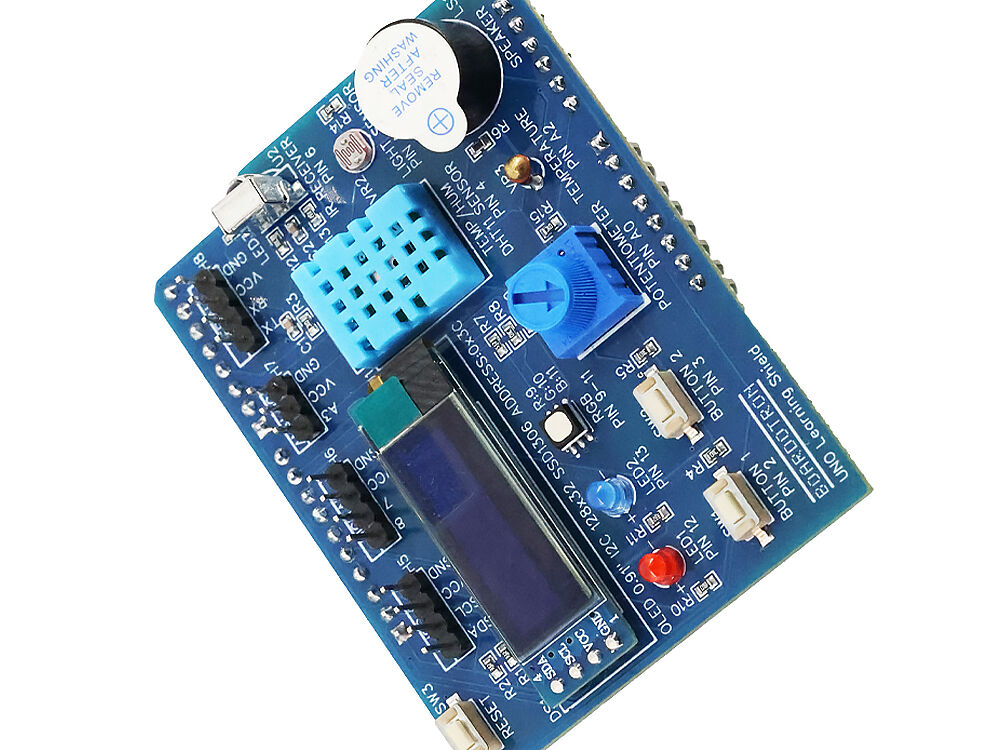
Surface-Mount Technology (SMT) is a PCB assembly method where electronic components (SMDs) are soldered directly to the surface of a printed circuit board (no drilled holes for component insertion, unlike through-hole technology).
Core details:
In the early days of electronics (1940s–1970s), through-hole technology was standard. Components had long leads inserted through board holes, then soldered to pads on the opposite side. This method:
As electronics evolved—driven by consumer demand for more features in smaller packages—through-hole mounting became a bottleneck. Manual assembly was time-consuming, error-prone, and costly for high-volume production.
SMT began emerging in the late 1970s and 1980s, pioneered by leading electronics manufacturers in Japan, the United States, and Europe.
By the 1990s, SMT had rapidly replaced through-hole as the dominant assembly technology in consumer, industrial, automotive, and aerospace electronics.
SMT enabled components to be much smaller, packed closer together, and mounted on both sides of a board—allowing for unparalleled product miniaturization.
SMT assembly processes are highly automatable, delivering:
Shorter interconnects and minimized lead inductance improved circuit performance, particularly at high frequencies and in RF applications.
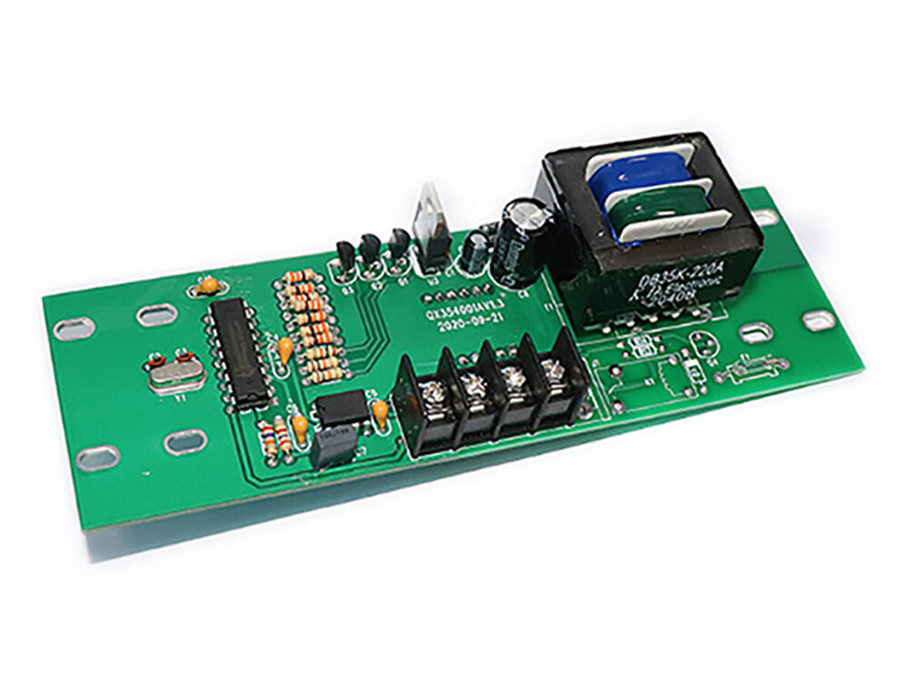
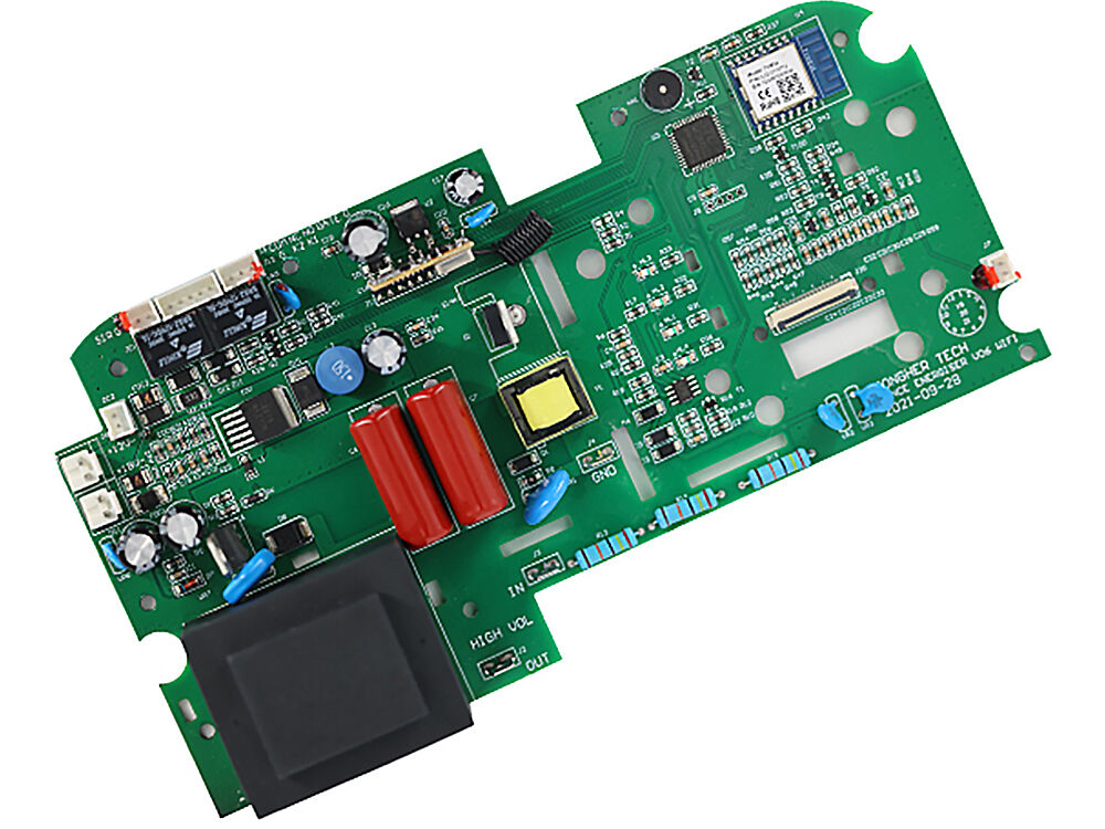
Thanks to SMT, today’s devices—like smartphones, tablets, medical instruments, and IoT gadgets—offer tremendous computing power in tiny forms. Most PCBs now use a mix of SMT and selective through-hole for robust or bulky parts.
Component Mounting: Components (SMDs) are placed directly onto the surface of the PCB without drilling holes.
Component Size and Density: Smaller component sizes allow for high-density layouts and miniaturized product designs.
Board Utilization: Enables component placement on both sides of the PCB, maximizing circuit complexity and functionality.
Assembly Process: Highly automated using pick-and-place machines and reflow soldering; enables high-speed, high-volume production.
Electrical Performance: Shorter interconnections reduce parasitic inductance/capacitance, supporting high-frequency and high-speed applications.
Mechanical Strength: Suitable for lightweight, low-power, and vibration-resistant designs, but may be less robust for heavy/large components.
Cost Efficiency: Lower assembly costs at scale due to automation and smaller board/part sizes.
Repair/Rework Difficulty: Challenging to manually solder, inspect, or repair due to tiny parts and dense placement.
Component Mounting: Leads of components are inserted through pre-drilled holes in the PCB and soldered on the reverse side.
Component Size and Density: Typically uses larger components with bigger footprints; less suitable for high-density/small designs.
Board Utilization: Components usually mounted on one side only, with leads running through the board.
Assembly Process: Often assembled manually or semi-automatically; suitable for prototyping, low-volume, and custom work.
Mechanical Strength: Solder joints provide strong mechanical anchoring—ideal for heavy, large, or high-stress parts (e.g., connectors, transformers, switches).
Electrical Performance: Longer interconnections may introduce more inductance and capacitance; less efficient for high-frequency circuits.
Cost Efficiency: Higher assembly cost for high volume due to slower production rates and greater material usage.
Repair/Rework: Easier to manually inspect, desolder, and replace components, making THT better for prototyping or repairable designs.
|
Feature |
Surface Mount Technology (SMT) |
Through-Hole Technology (THT) |
|
Mounting Method |
On PCB surface, no holes needed |
Component leads through holes |
|
Component Size |
Small (SMD), high-density |
Larger, low to medium density |
|
Assembly |
Highly automated, fast |
Manual or semi-automatic, slower |
|
Repairability |
Difficult, needs special tools |
Easier, suitable for repair/prototyping |
|
Mechanical Strength |
Less for heavy parts |
Excellent for heavy, high-stress parts |
|
Board Sides Used |
Both |
Mainly one (component side) |
|
Cost (Large Volume) |
Lower after setup |
Higher due to more labor/space needed |
|
Electrical Performance |
Superior at high frequencies |
Less optimal for high frequency |
|
Feature |
Through-Hole Technology (THT) |
Surface Mount Technology (SMT) |
|
Mounting Method |
Components go through drilled holes |
Components mounted on PCB surface |
|
Component Size |
Larger, long leads |
Small (SMD), short/no leads |
|
Board Sides Used |
One side (usually) |
Both sides possible |
|
Assembly Process |
Manual or semi-auto, slower |
Highly automated, faster |
|
Density/Size |
Lower density, larger PCBs |
High density, smaller PCBs |
|
Mechanical Strength |
Strong for large parts |
Best for small, light parts |
|
Repairability |
Easier |
More difficult, needs special tools |
|
Electrical Performance |
Less optimal for high frequency |
Superior for high frequency |
|
Cost (Mass Prod.) |
Higher |
Lower |
|
Factor |
Surface Mount Technology (SMT) |
Through-Hole Technology (THT) |
|
Component Size |
Small, high-density |
Large, lower density |
|
Mechanical |
Less robust for heavy components |
Strong for stress/heavy parts |
|
Performance |
Best for high-speed/frequency |
Adequate for low-speed/power |
|
Assembly Speed |
High-speed, automated |
Slower, manual/semi-auto |
|
Repair/Rework |
Difficult, needs expertise |
Easy, ideal for prototyping |
|
Board Sides |
Double-sided possible |
Mostly single-sided |
1. High-Density, Miniaturized Designs
2. High-Volume Production
3. Double-Sided or Multilayer PCBs
4. High-Speed or High-Frequency Circuits
5. Automated PCB Assembly
6. Reduced Manufacturing Cost at Scale
7. Modern Consumer, Medical, and Automotive Electronics
|
Soldering Technique |
Usage Context |
Advantages |
|
Reflow Soldering |
Mass SMT assembly |
Highly automated, reliable |
|
Wave Soldering |
Mixed tech, thru-hole |
Fast for some hybrid assemblies |
|
Hand Soldering |
Prototyping, repair |
Flexible, low volume |
|
Selective Soldering |
Special mixed boards |
Precision, protects sensitive parts |
|
Vapor Phase Soldering |
High-reliability/complex |
Uniform heating, low defects |
Surface mount device (SMD) packages are standardized formats for mounting electronic components directly onto the surface of printed circuit boards (PCBs) using surface mount technology (SMT). Proper selection of SMD packages is crucial for optimizing board density, performance, and manufacturability.
 Hot News
2026-01-17
2026-01-16
2026-01-15
2026-01-14
2026-01-13
2026-01-12
2026-01-09
2026-01-08