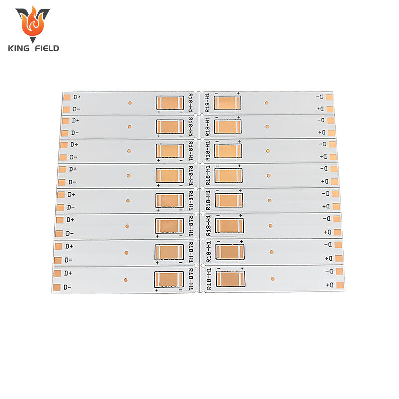
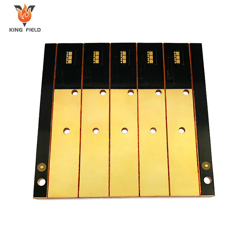
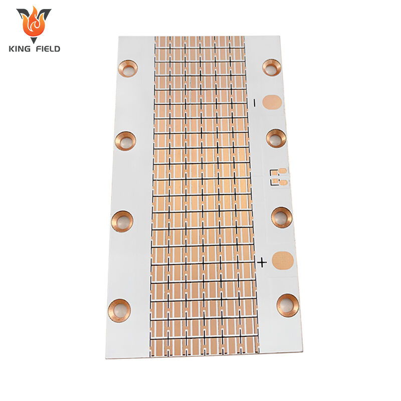
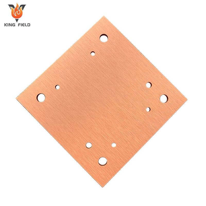
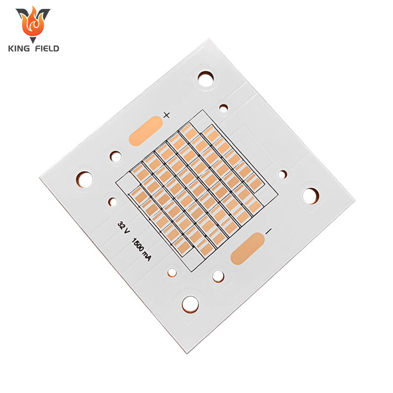
Heavy Copper PCB
High-power Heavy Copper PCBs for industrial/automotive/medical applications. 3oz-20oz copper thickness, excellent current carrying capacity & thermal conductivity. 24h prototyping, fast delivery, DFM support & quality testing.
✅ 3oz-20oz thick copper
✅ Superior thermal management
✅ High-power device compatibility
Description
What is a Heavy Copper PCB?
Heavy Copper PCB, also known as thick copper PCB, is a special type of PCB with a copper foil thickness of ≥2oz. Common specifications range from 2oz to over 10oz. Its core features are stronger current-carrying capacity, heat dissipation performance and mechanical strength. Special electroplating and etching processes are required for production to ensure the uniformity and adhesion of the thick copper layer. Compared with ordinary PCBS, heavy copper PCBS have a stronger current-carrying capacity, excellent heat dissipation, and higher process difficulty. They are mainly applied in scenarios such as power equipment, industrial control frequency converters, new energy vehicle electronic control systems, and medical equipment power modules that require large current transmission, high power output, or strong heat dissipation. Ordinary PCBS are mostly suitable for consumer electronics and low-power devices.
The core advantages of thick copper pcb focus on their adaptability to high-current and high-power scenarios, which are specifically reflected in the following aspects:
· Super strong current-carrying capacity:
The thick copper layer (≥2oz) can carry tens to hundreds of amperes of large current, which is far superior to ordinary PCBS. It can meet the current transmission requirements of high-power products such as power equipment and new energy vehicle electronic control systems, and avoid line heating and burning caused by current overload.
· Excellent heat dissipation performance:
Copper has excellent thermal conductivity. A thicker copper layer is an excellent heat conductor, and its heat dissipation efficiency is much higher than that of standard PCBS. The thickened copper layer can quickly conduct the heat generated during circuit operation, effectively reducing the surface temperature of the board, minimizing the damage to components and circuits caused by thermal aging, and enhancing the stability and service life of the product.
· Higher mechanical strength:
Another key advantage of high-copper PCBS lies in their higher mechanical strength. The thick copper layer enhances the physical toughness of the PCB, making it more resistant to bending and impact, and thus more capable of withstanding physical stresses such as bending, vibration and mechanical shock. It can adapt to harsh working conditions with frequent vibrations such as industrial control equipment and vehicle-mounted environments, reducing the risk of line breakage.
· Stable electrical conductivity reliability
The thick copper layer reduces the resistance loss during current transmission, lowers the voltage drop, and ensures the stability of circuit signal and power transmission. It is particularly suitable for medical equipment and precision industrial control systems with high requirements for power supply accuracy.
· Integrated design support:
It can achieve an integrated layout of high-current circuits and precise signal circuits, reducing the need for external heat sinks, shunts and other components, simplifying the product structure and improving space utilization.
· Prolong life
Higher current-carrying capacity, better heat dissipation management and stronger mechanical strength jointly extend the service life of thick copper pcb. These PCBS are not prone to thermal or mechanical damage, thus ensuring their normal operation for a longer time. This reliability is of vital importance in application fields where maintenance or replacement is difficult and costly, such as aerospace or industrial environments.
| Technical specifications | Standard PCB | Heavy copper PCB | |||
| Thickness of copper foil | It is usually about 1 ounce per square foot | It is usually 3 ounces per square foot to 10 ounces per square foot or higher | |||
| Current-carrying capacity | Weak, only supports small currents (usually ≤10A) | It is strong and can carry large currents ranging from tens to hundreds of amperes | |||
| Heat dissipation performance | Generally, heat conduction is slow | Excellent, the thick copper layer quickly dissipates heat | |||
| Mechanical strength | Ordinary, with limited resistance to bending and impact | Higher, the thickened copper layer enhances physical toughness | |||
| Resistance loss | It is relatively high and prone to voltage drop | Lower, more stable power/signal transmission | |||
| Process difficulty | Conventional processes are technologically mature and have low costs | It requires a dedicated electroplating/etching process and has a relatively high cost | |||
| Applicable scenarios | Consumer electronics (mobile phones/computers), low-power devices | High-power equipment, electronic control systems for new energy vehicles, medical power modules | |||
| Design complexity | Simple, no special heat dissipation/current-carrying design required | Complex circuit layout and impedance control that require matching thick copper layers | |||
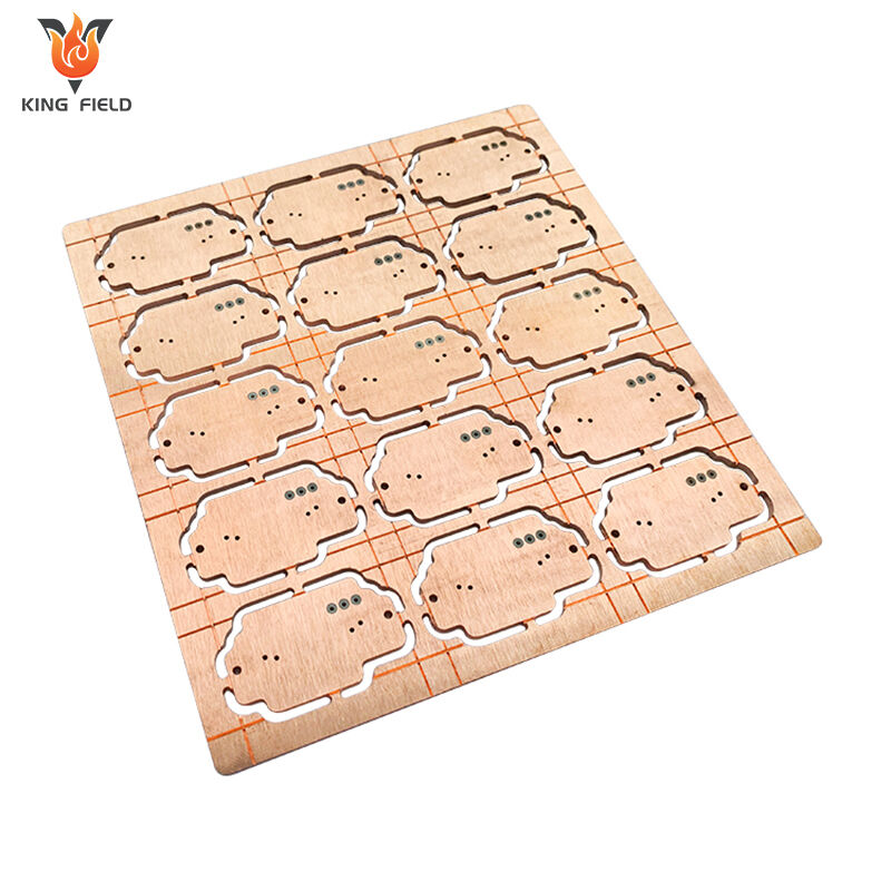
Manufacturing Capabilities
| PCB Manufacturing Capability | |||||
| ltem | Production capability | Min space for S/M to pad, to SMT | 0.075mm/0.1mm | Homogeneity of Plating Cu | z90% |
| Layer Count | 1~40 | Min space for legend to pad/ to SMT | 0.2mm/0.2mm | Accuracy of pattern to pattern | ±3mil(±0.075mm) |
| Production size(Min & Max) | 250mmx40mm/710mmx250mm | Surface treatment thickness for Ni/Au/Sn/OSP | 1~6um /0.05~0.76um /4~20um/ 1um | Accuracy of pattern to hole | ±4mil (±0.1mm ) |
| Copper thickness of lamination | 1/3 ~ 10z | Min size E- tested pad | 8 X 8mil | Min line width/space | 0.045 /0.045 |
| Product board thickness | 0.036~2.5mm | Min space between tested pads | 8mil | Etching tolerance | +20%0.02mm) |
| Auto-cutting accuracy | 0.1mm | Min dimention tolerance of outline (outside edge to circuit) | ±0.1mm | Cover layer alignment tolerance | ±6mil (±0.1 mm) |
| Drill size(Min/Max/hole sizetolerance) | 0.075mm/6.5mm/±0.025mm | Min dimention tolerance of outline | ±0.1mm | Excessive adhesive tolerancefor pressing C/L | 0.1mm |
| Warp&Twist | ≤0.5% | Min R corner radius of outline(inner filleted corner) | 0.2mm | Alignment tolerance forthermosetting S/M and UV S/M | ±0.3mm |
| maximum aspect Ratio(thickness/hole diameter) | 8:1 | Min space golden finger to outline | 0.075mm | Min S/M bridge | 0.1mm |
Inspection and Testing
Due to the thick copper layer and special application scenarios, the inspection and testing of heavy copper printed circuit boards (thick copper PCBS) need to cover three major dimensions: process quality, electrical performance, and reliability. The core contents are as follows:
Inspection of appearance and process defects
· Copper layer quality: Check whether the thick copper layer has peeling, cracking, oxidation, and whether there are burrs at the edge of the line due to uneven etching (it needs to comply with IPC-A-600 standard);
· Pads and vias: Verify the flatness and adhesion of the pads, whether the copper layer thickness on the vias' walls meets the standards, and whether there are any voids or misaligned holes.
· Board surface deformation: Measure the warpage of the PCB (thick copper PCBS are prone to warpage due to copper layer stress, which should be controlled within 0.75%), and check for delamination or bubbles.
· Dimensional accuracy: Check the key dimensions such as line width, spacing, and hole diameter to ensure they are consistent with the design drawings.
Electrical performance test
· Conduction and Insulation test (Hi-Pot test) : The insulation between lines is detected by a high-voltage insulation tester to prevent breakdown caused by insufficient spacing between thick copper layers. Verify conductivity and troubleshoot open circuit and short circuit faults;
· Current-carrying capacity test: Apply the rated current under simulated actual working conditions, monitor the temperature rise of the circuit, and confirm that there is no risk of overheating or melting.
· Impedance testing: Use an impedance analyzer to detect the characteristic impedance of the high-frequency signal line to ensure that the influence of the thick copper layer on the impedance meets the design requirements (error ≤±10%);
· Voltage drop test: Measure the line voltage drop under high current transmission to verify the low resistance advantage of the thick copper layer and avoid voltage loss affecting equipment performance.
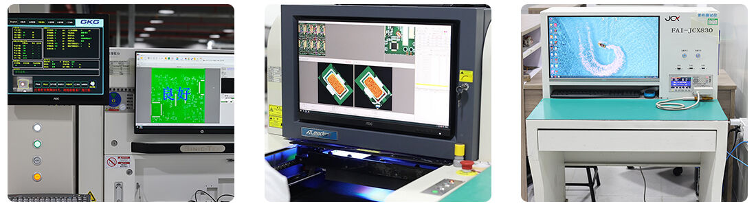
Automatic Optical Inspection (AOI)
Automatic Optical Inspection (AOI) utilizes advanced imaging technology to detect defects that may not be visible to the naked eye.
· High-resolution imaging: The AOI system captures high-resolution images of the PCB and compares them with design specifications.
· Defect detection: This system can automatically identify issues such as short circuits, open circuits, thinning of traces, and misalignment.
· Precision: AOI offers high precision, ensuring that even the tiniest defects can be detected and resolved.
Reliability test
· Thermal cycling test: Cycle test within the temperature range of -40 ℃ to 125℃ (≥1000 times) to check the bonding stability of the thick copper layer with the substrate and pads, without delamination or cracking.
· Thermal shock test: Quickly switch between high and low temperature environments (temperature difference ≥80℃) to verify the PCB's resistance to sudden temperature changes, suitable for harsh scenarios such as automotive and industrial control.
· Vibration and mechanical strength testing: Simulate the vibration (frequency 5~500Hz) and impact during transportation and use to check whether the thick copper circuit is broken and whether the vias have fallen off.
· Corrosion resistance test: Verify the oxidation resistance and corrosion resistance of the thick copper layer through salt spray test (neutral salt spray, 48 to 96 hours) or damp heat test (85℃/85% RH, 1000 hours).
· Soldering reliability test: After completing SMT/through-hole soldering, check the bonding strength between the solder joints and the thick copper pads, and ensure there is no false soldering or de-soldering.
Special performance verification
· Heat dissipation performance test: The temperature distribution of the PCB under full-load conditions was detected by a thermal imager to verify the heat dissipation effect of the thick copper layer.
· Flame retardancy test: For high-power application scenarios, the flame retardancy grade of the PCB is tested in accordance with UL94 standards (at least reaching V-0 level);
· Adhesion test: A hundred-grid test or tensile test is adopted to verify the adhesion between the thick copper layer and the substrate (≥1.5N/mm).
Applications of Heavy Copper PCBs
Thick copper printed circuit boards, with their strong current-carrying capacity, excellent heat dissipation and high mechanical strength, are mainly applied in fields that require large current transmission, high power output or harsh working conditions. The core scenarios are as follows:
In the field of new energy vehicles
Core components: On-board charger, battery management system, motor controller, DC/DC converter, charging pile module.
Application reason: It needs to carry large currents, withstand alternating high and low temperatures and vibrations. Thick copper PCBS can ensure stable power transmission and efficient heat dissipation, and are suitable for the harsh environment of vehicles.
Industrial control and power equipment
Core components: frequency converter, servo driver, UPS power supply, industrial power module, high-voltage distribution cabinet control board, main control board of electric welding machine.
Application reason: Industrial control equipment often requires high power output. Thick copper PCBS can reduce line resistance loss, prevent overheating, and at the same time resist mechanical vibration and electromagnetic interference, enhancing equipment reliability.
The field of medical equipment
Core components: Medical power supplies, ventilator power modules, control boards for electrosurgical instruments.
Application reason: Medical equipment has extremely high requirements for power supply stability and safety. Thick copper PCBS can achieve low voltage drop, high heat dissipation, and meet the strict insulation and withstand voltage standards of the medical industry.
Aerospace and military industry fields
Core components: Airborne power supply system, radar launch module, missile control board, satellite power supply unit.
Application reason: To adapt to extreme temperatures, strong vibrations and radiation environments, the high mechanical strength and stable electrical performance of thick copper PCBS can ensure the normal operation of equipment under harsh conditions.
High-power consumer and commercial equipment
Core components: Energy storage inverter, photovoltaic inverter, high-power home appliance control board (such as induction cookers, electric ovens), data center power module.
Application reason: High-power equipment generates a lot of heat and has a high current. Thick copper PCBS can quickly dissipate heat, prevent circuit overload and burnout, and extend the service life of the equipment.
The field of rail transit
Core components: Train traction converter, track power supply system, signal control module.
Application reason: Rail transit equipment needs to withstand long-term vibration, high and low temperatures, and frequent start-stop large current impacts. The current-carrying capacity and mechanical reliability of thick copper PCBS can meet this requirement.