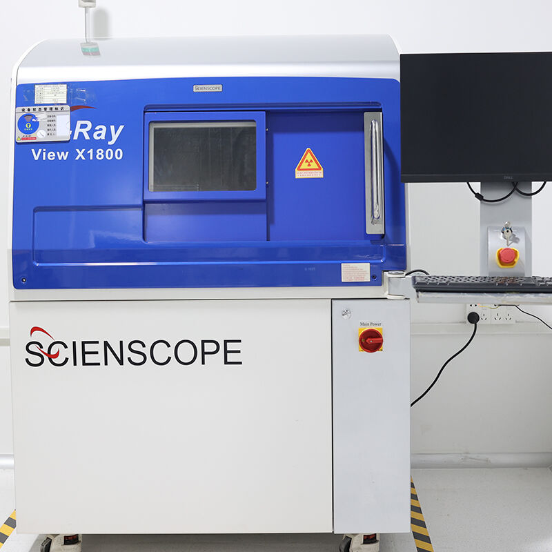
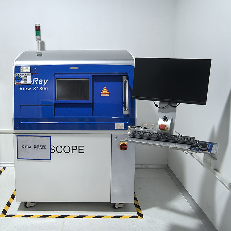
X-RAY
High-precision X-Ray inspection for PCB/PCBA assemblies—detect hidden defects in BGA, QFN, CSP, and micro-components. Ensures solder joint integrity, voiding, and component alignment with IPC-A-610 compliance.
✅ Non-destructive BGA/QFN/CSP inspection
✅ Solder void & joint integrity analysis
✅ IPC-A-610 compliant results
✅ Fast, detailed inspection reports
✅ Reduces production failure risks
Description
What is Automated X-ray Inspection?
PCB X-ray inspection, also known as automated X-ray inspection, is widely used in various industries, from medical to aerospace manufacturing, for identifying manufacturing errors. It is particularly common in PCB inspection because X-rays provide an excellent method for testing PCB quality and detecting hidden defects without damaging the circuit board.
As electronics get smaller and more complex, with components like BGAs and QFNs hiding solder joints under packages, Automated X-ray Inspection has become an indispensable tool in the assembly workflow.
Key Advantages Over AOI
| AXI Advantages | AOI Limitations Addressed | ||||
| Detects hidden internal defects | Only inspects surface-level features; cannot see under components | ||||
| Non-destructive testing—no damage to PCBA during inspection | Same as AOI, but AXI’s penetration capability expands inspection scope | ||||
| High accuracy for fine-pitch, miniaturized components | Struggles with components that cover solder joints or have fine pitches | ||||
| Enables 3D tomography for layered inspection of multi-layer PCBs | Limited to 2D or pseudo-3D surface analysis |
Key Application Scenarios in PCB/PCBA Production
Post-Reflow Inspection for Hidden Components
The most common use case—inspecting solder joints of BGA, QFN, CSP, and flip-chip devices where solder connections are under the component body and inaccessible to AOI.
High-Reliability Industry Testing
Mandatory for automotive, aerospace, medical, and military electronics. For example, AXI verifies BGA solder voids in automotive ECUs (to meet IATF 16949 standards) and ensures zero defects in medical device PCBA (complying with ISO 13485).
Multi-Layer PCB Internal Inspection
Detects internal defects like interlayer short circuits, via misalignment, and improper copper trace placement in complex multi-layer PCBs.
Failure Analysis
Used in root-cause analysis for field-failed PCBA to identify hidden defects that are not visible via visual inspection.
2D AXI vs. 3D AXI
Similar to AOI, AXI is categorized into two types based on imaging capability:
· 2D AXI: Captures a single planar X-ray image, suitable for basic inspection of low-density PCBs. Cost-effective but may have overlapping image artifacts.
· 3D AXI (X-ray Tomography): Uses computed tomography to generate layered 3D images of the PCBA. Eliminates overlapping artifacts and enables precise measurement of solder joint volume/void ratio—ideal for high-density, high-precision electronics.
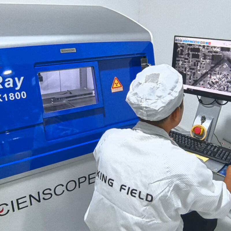
How Does X-Ray Inspection System Work?
An X-ray inspection system (commonly referred to as Automated X-ray Inspection, AXI) is a non-destructive testing (NDT) technology that penetrates PCB/PCBA assemblies to detect hidden internal defects. Unlike AOI (which only captures surface visuals), AXI leverages X-ray radiation’s ability to pass through materials of varying densities, making it the gold standard for inspecting enclosed components like BGA, QFN, and flip chips.
The working process of an X-ray inspection system can be broken down into 5 core sequential steps:
Step 1: System Calibration & Reference Setup
Before inspection, the system is configured to match the PCBA’s design specifications:
· Import Reference Data: Load the PCB’s CAD file or a golden sample (defect-free PCBA) image to set the benchmark for acceptable solder joint shape, volume, and component positioning.
· Adjust X-Ray Parameters: Fine-tune X-ray dose, voltage, and current based on the PCBA’s thickness and component density. Thicker boards or denser components require higher voltage to ensure sufficient penetration.
· Set Defect Tolerance Thresholds: Define acceptable ranges for defects like solder void size or solder ball displacement to avoid false alarms.
Step 2: X-Ray Emission & Penetration
The core of the system is the X-ray generator, which emits a controlled beam of low-dose X-rays toward the PCBA under inspection:
The PCBA is placed on a precision conveyor or stage, ensuring stable positioning during scanning.
X-rays pass through the PCBA. Materials absorb X-rays differently based on their density:
· High-density materials: Absorb more X-rays, appearing as dark areas in the final image.
· Low-density materials: Absorb fewer X-rays, appearing as light areas in the final image.
For 3D AXI systems, the PCBA or X-ray source rotates at multiple angles to capture multi-directional penetration data.
Step 3: Image Capture & Signal Conversion
A high-sensitivity X-ray detector (located on the opposite side of the X-ray source) captures the attenuated X-ray signals after they pass through the PCBA:
The detector converts the X-ray energy into electrical signals, which are then translated into digital grayscale images.
· For 2D AXI: A single planar image is generated, showing the overlapping internal structure of the PCBA.
· For 3D AXI (X-ray tomography): Multiple 2D images from different angles are stitched together using reconstruction algorithms to create a layered 3D model of the PCBA—eliminating image overlap and enabling cross-sectional views.
Step 4: Image Analysis & Defect Detection
This is the intelligent core of the system, where software algorithms analyze the captured images against the pre-set reference:
· 2D AXI Analysis: Compares the grayscale distribution of the PCBA image to the golden sample. Anomalies like dark spots (excess solder) or bright spots are flagged as potential defects.
· 3D AXI Analysis: Uses the 3D model to measure precise dimensions. It can distinguish between minor variations and critical defects.
· Defect Classification: The system sorts defects by severity:
Critical: Solder bridges between BGA pins, large voids, missing solder balls.
Major: Slight solder ball displacement, small voids.
Minor: Cosmetic issues with no impact on functionality.
Step 5: Result Output & Actionable Reporting
After analysis, the system generates clear, traceable results for production teams:
· Defect Visualization: Marks the exact location of defects on the PCBA image or 3D model for easy identification.
· Detailed Reporting: Creates logs with defect type, location, severity, and compliance status. This data is stored for process optimization and quality traceability.
· Post-Inspection Routing: The PCBA is automatically directed to a repair station for defect correction, or passed to the next production stage if no defects are detected.