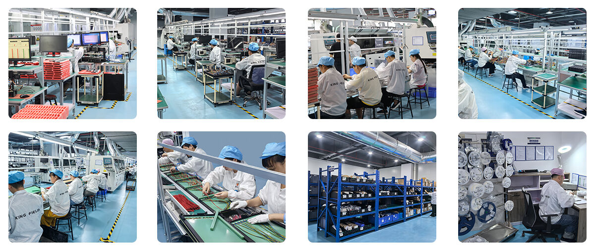
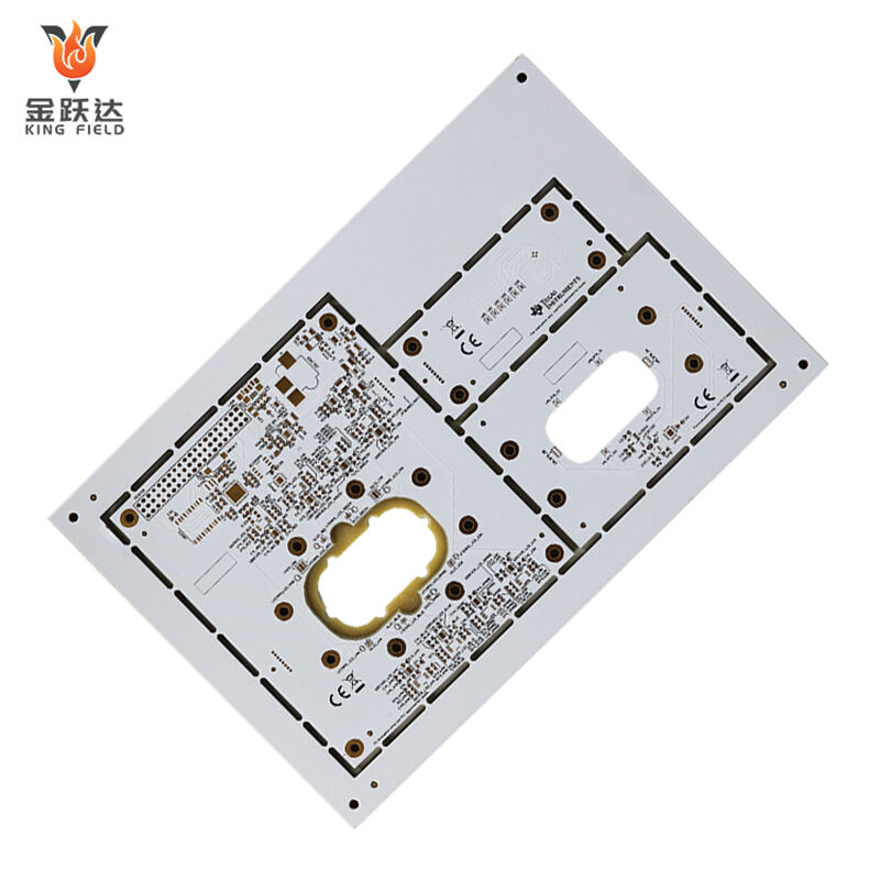
PCB Prototype
Rapid, Precision PCB Prototyping for medical, industrial, automotive & consumer electronics. 24h fast turnaround, multi-layer support (2-40 layers), compatible with all substrate types (FR4/Rogers/ceramic) & surface finishes. DFM optimization, strict quality checks, and seamless scaling to mass production accelerate your R&D cycle.
✅ 24h quick turnaround
✅ Multi-layer (2-40L) & multi-substrate support
✅ DFM analysis & quality validation
✅ R&D to mass production seamless transition
Description
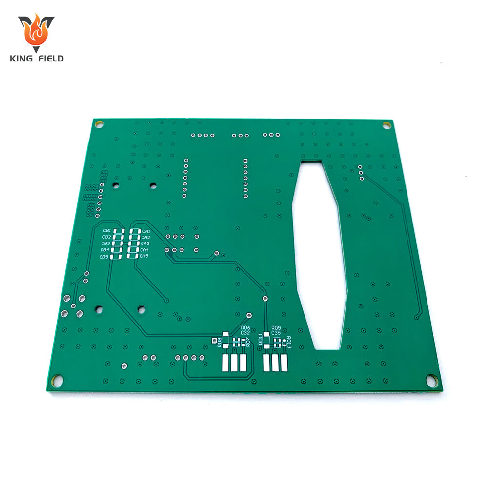
What is a PCB prototype?
A prototype circuit board refers to a small batch of PCBs produced before mass production to verify circuit design, manufacturing feasibility, and functional stability. It is a crucial intermediate step in the PCB product lifecycle, from design to mass production. The core purpose is to identify and correct design flaws and test process compatibility, preventing large-scale failures or cost losses during mass production.
Prototype printed circuit boards, as a core component of the electronic product development process, offers key advantages in three main areas: risk control, development efficiency, and cost optimization, as detailed below:
Early detection of design flaws reduces mass production risks.
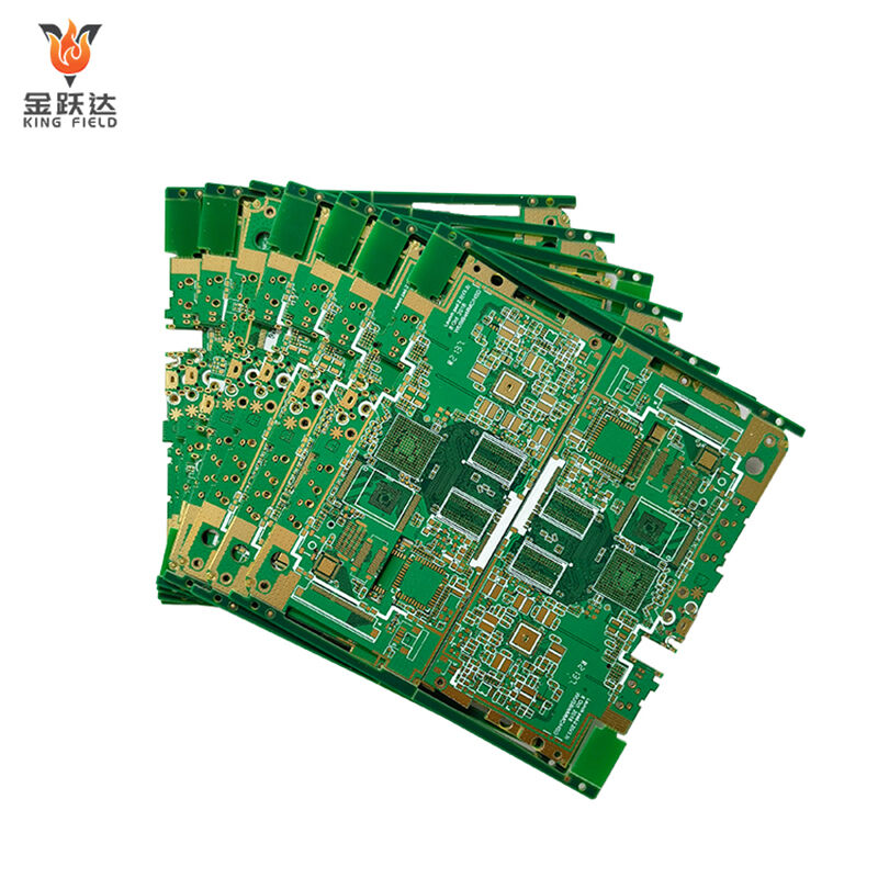
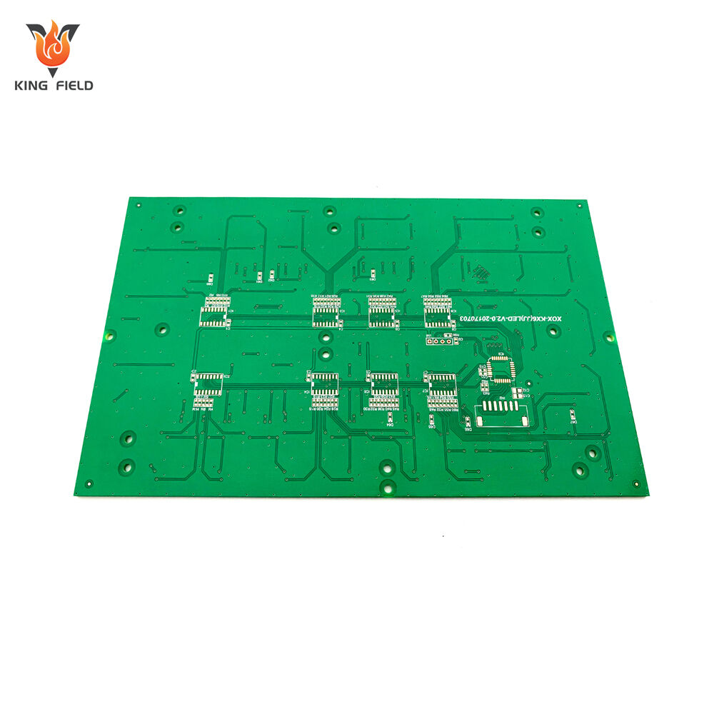
Prototype board pcb can accurately replicate the circuit, layout, and process parameters of the design plan on a 1:1 scale, enabling precise identification of hidden problems during the R&D phase:
· Electrical defects: such as short circuits/open circuits, impedance mismatch, signal interference, etc.;
· Structural conflicts: such as crowded component layout, mismatched pad sizes, and deviations in mounting hole positions;
· Process difficulties: such as the difficulty of processing special substrates and the feasibility of drilling/plating processes.
If these problems are only discovered during the mass production stage, it will lead to mass scrapping, delivery delays, and even damage to brand reputation. Prototype verification can avoid more than 90% of mass production risks.
Accelerate R&D iteration and shorten product launch cycles:
· Fast delivery: prototype board pcb support expedited manufacturing, significantly faster than mass production cycles, allowing for rapid verification of design solutions and multiple iterations for optimization;
· Flexible modifications:
Design modifications during the prototyping phase are extremely cost-effective, while modifying designs during mass production requires re-tooling and adjusting the production line, costing tens of times more than prototyping;
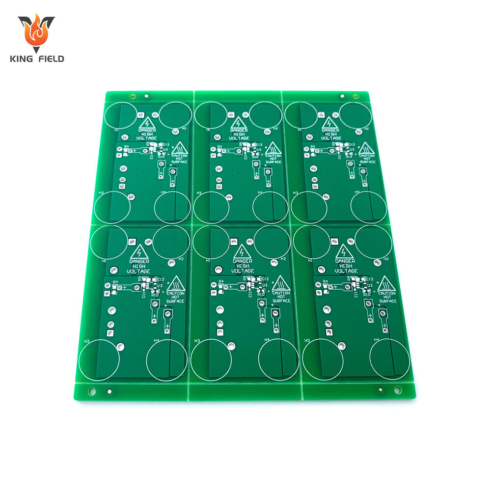
· Parallel verification: Multiple prototypes with different designs can be manufactured simultaneously to compare performance differences and quickly determine the optimal solution.
Control R&D costs and avoid ineffective investments:
· Small-batch prototyping: Only 1-50 prototypes are needed. Although the cost per unit is high, the overall investment is far lower than the losses incurred from mass production and subsequent scrapping;
· Process pre-validation: For special processes, prototype testing can verify the manufacturer's process capabilities, avoiding the risk of collaboration issues due to the manufacturer's inability to meet process standards during mass production;
· Customer validation: Prototype samples can be produced for customer testing to confirm in advance whether the product functions meet requirements, avoiding rework caused by changes in customer requirements after mass production is completed.
Improving Product Reliability and Optimizing User Experience
· Through repeated testing of prototypes , the PCB's heat dissipation design, anti-interference capabilities, and structural stability can be optimized, thereby improving the reliability and lifespan of the final product;
· For fields with high safety requirements, such as consumer electronics and automotive electronics, prototype verification is a crucial prerequisite for product certification.
Flexible Adaptation to Customized Needs
· PCB prototyping supports non-standard designs, without the limitations of mass production standardization. This meets the customized R&D needs of niche applications and high-end equipment.
· For startups or research institutions, prototyping eliminates the pressure of minimum order quantities associated with mass production, allowing them to focus on technology verification and product innovation.
Proto board pcb are used throughout the entire process of electronic product research, development, testing, and certification, focusing primarily on "verification and trial-and-error" scenarios. Specific application areas and scenarios include:
Consumer Electronics Development
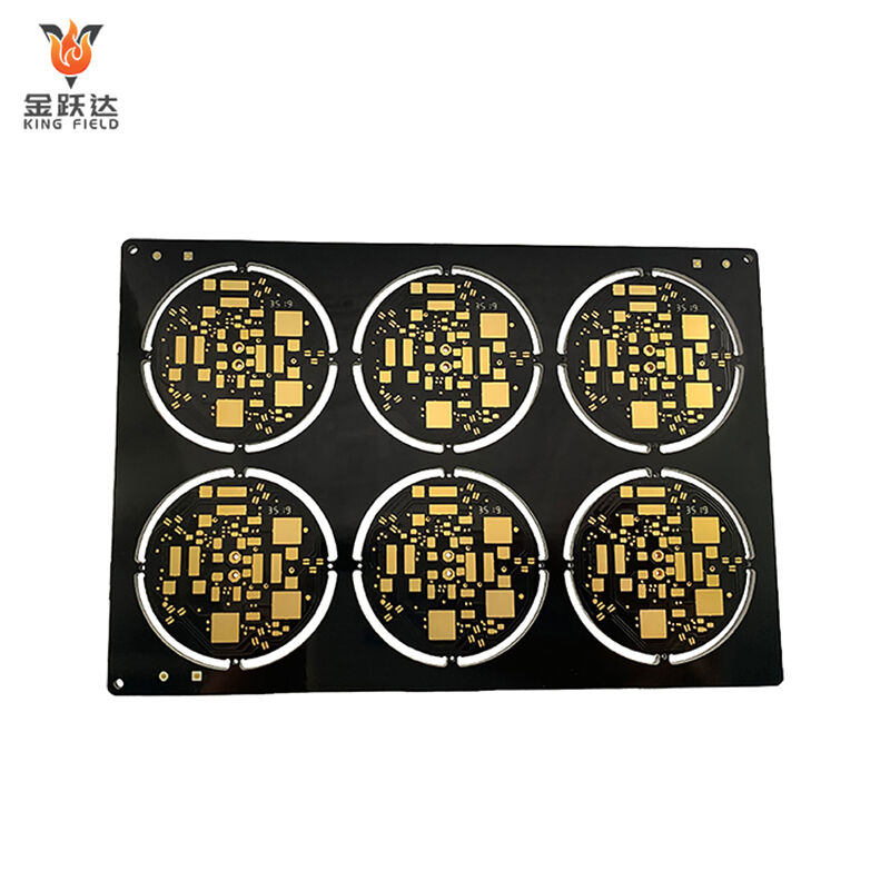
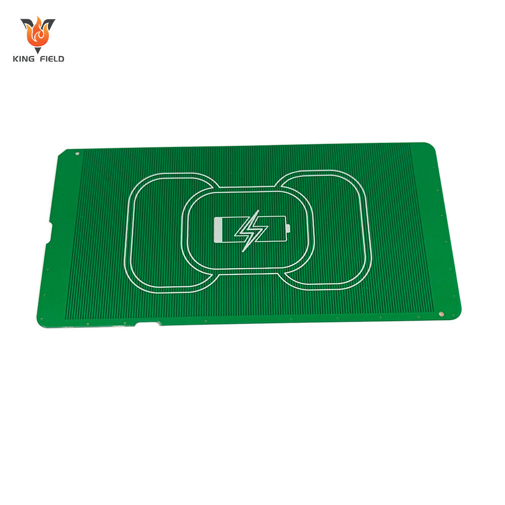
· Scenarios: Prototype verification of smartphone motherboards, smart home control boards, Bluetooth headphone PCBs, and smart wearable device (watch/bracelet) circuit boards;
· Function: Testing circuit functions, component compatibility, and structural adaptability, and identifying design flaws in advance.
Industrial Control and Internet of Things
· Scenarios: Prototyping of PLC modules, industrial sensor PCBs, IoT gateway circuit boards, and charging pile control boards;
· Function: Verifying reliability in extreme environments, communication protocol stability, and electromagnetic interference resistance, ensuring long-term stable operation in industrial settings.
Automotive Electronics Development
· Scenarios: Automotive radar PCBs, battery management system (BMS) prototypes, body control module (BCM) prototypes, and autonomous driving sensor circuit boards;
· Function: Testing performance under harsh automotive conditions, electromagnetic compatibility, and pre-verification for automotive industry certifications such as AEC-Q200.
Medical Equipment Development
· Scenarios: Prototypes of medical monitor PCBs, portable diagnostic equipment circuit boards, and surgical instrument control boards;
· Function: Verifying circuit safety, and data accuracy, meeting the stringent certification standards for medical devices.
Aerospace and Defense
· Scenarios: Satellite communication PCBs, airborne radar prototypes, and military equipment control board prototypes;
· Function: Testing performance in extreme environments such as radiation resistance, high temperature resistance, and low pressure, and verifying high-reliability designs. University Research and Maker Projects
· Scenarios: Student electronic competition projects, laboratory research projects, maker DIY devices;
· Benefits: Low-cost verification of creative designs, rapid iteration and optimization of solutions, without the pressure of mass production costs.
Manufacturing Capabilities
| Rigid RPCB Manufacturing Capability | |||||
| Item | RPCB | HDI | |||
| minimum linewidth/linespacing | 3MIL/3MIL(0.075mm) | 2MIL/2MIL(0.05MM) | |||
| minimum hole diameter | 6MIL(0.15MM) | 6MIL(0.15MM) | |||
| minimum solder resist opening (single-side) | 1.5MIL(0.0375MM) | 1.2MIL(0.03MM) | |||
| minimum solder resist bridge | 3MIL(0.075MM) | 2.2MIL(0.055MM) | |||
| maximum aspect Ratio (thickness/hole diameter) | 0.417361111 | 0.334027778 | |||
| impedance control accuracy | +/-8% | +/-8% | |||
| finished thickness | 0.3-3.2MM | 0.2-3.2MM | |||
| maximum board size | 630MM*620MM | 620MM*544MM | |||
| maximum finished copper thickness | 6OZ(210UM) | 2OZ(70UM) | |||
| minimum board thickness | 6MIL(0.15MM) | 3MIL(0.076MM) | |||
| maximum layer | 14 layer | 12 layer | |||
| Surface treatment | HASL-LF、OSP 、Immersion Gold、 Immersion Tin 、Immersion Ag | Immersion Gold、OSP、selectiveimmersion gold、 | |||
| carbon print | |||||
| Min/max laser hole size | / | 3MIL / 9.8MIL | |||
| laser hole size tolerance | / | 0.1 | |||