PCB Design & Layout
Professional PCB Design & Layout services for medical, industrial, automotive & consumer electronics. Expert team delivers DFM-optimized designs, fast turnaround, and seamless alignment with your R&D goals. From schematic capture to gerber files—ensure manufacturability, signal integrity, and on-time production.
Description
PCB Design and Layout
Precision PCB Design and Layout Solutions:
Providing engineering excellence for your electronic products, including cutting-edge design, rapid prototyping, and comprehensive production support.
Our PCB Design Services
Comprehensive solutions from concept to production, tailored to your specific requirements.
|
Design Review and Optimization
|
PCB Layout Design Precise layout considering signal integrity, power distribution, and manufacturability constraints.
|
Prototyping and Testing Rapid prototyping services with comprehensive testing to ensure your design meets all specifications.
|
Advantages
Our Advantages
We possess advanced design capabilities and can handle complex PCB projects across various industries.
|
1. One-stop solution service: We provide one-stop solution services covering the entire process from concept to final product manufacturing, including shell design, hardware development, software programming, product testing, etc. |
2. Professional Design Team: Our PCB design team consists of experienced engineers who are proficient in circuit design, layout, and manufacturing best practices, and are familiar with various commonly used design software. |
3. Rapid Design and Delivery: Our strong design capabilities ensure the shortest possible PCB design cycle, with some projects completed in as little as 24 hours to meet your design requirements. |
 |
 |
 |
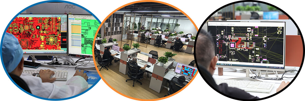
Advanced Technologies and Capabilities
Our state-of-the-art design tools and engineering expertise enable us to handle the most complex projects with precision and efficiency PCB project
High-density interconnect (HDI)
The advanced HDI board design capabilities with microvias enable smaller form factor and higher component density.
High-speed design
The engineers possess expertise in high-speed design of signal integrity, as well as advanced simulation and analysis capabilities.
Manufacturing capacity
| PCB Manufacturing Capability | |||||
| ltem | Production capability | Min space for S/M to pad, to SMT | 0.075mm/0.1mm | Homogeneity of Plating Cu | z90% |
| Layer Count | 1~40 | Min space for legend to pad/ to SMT | 0.2mm/0.2mm | Accuracy of pattern to pattern | ±3mil(±0.075mm) |
| Production size(Min & Max) | 250mmx40mm/710mmx250mm | Surface treatment thickness for Ni/Au/Sn/OSP | 1~6um /0.05~0.76um /4~20um/ 1um | Accuracy of pattern to hole | ±4mil (±0.1mm ) |
| Copper thickness of lamination | 1\3 ~ 10z | Min size E- tested pad | 8 X 8mil | Min line width/space | 0.045 /0.045 |
| Product board thickness | 0.036~2.5mm | Min space between tested pads | 8mil | Etching tolerance | +20%0.02mm) |
| Auto-cutting accuracy | 0.1mm | Min dimention tolerance of outline (outside edge to circuit) | ±0.1mm | Cover layer alignment tolerance | ±6mil (±0.1 mm) |
| Drill size(Min/Max/hole sizetolerance) | 0.075mm/6.5mm/±0.025mm | Min dimention tolerance of outline | ±0.1mm | Excessive adhesive tolerancefor pressing C/L | 0.1mm |
| Min percent for CNC slot length and width | ≤0.5% | Min R corner radius of outline(inner filleted corner) | 0.2mm | Alignment tolerance forthermosetting S/M and UV S/M | ±0.3mm |
| maximum aspect Ratio(thickness/hole diameter) | 8:1 | Min space golden finger to outline | 0.075mm | Min S/M bridge | 0.1mm |

