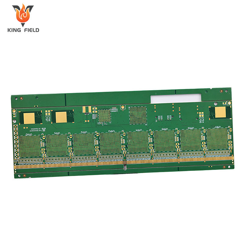
Multilayer PCB fabrication is the leading technology that supports the development of advanced electronics, allowing the integration of compact and high-performance gadgets which have wide applications in consumer electronics, aerospace, and medical instrument industries. While single- or double-layer PCBs refer to one or two layers of copper only, multilayer PCBs are three or more layers of copper stacked and separated with insulating materials that make possible more complicated circuit routing, higher component density, and better electrical performance. Understanding the principal steps of multilayer PCB fabrication will make designers, engineers, and buyers more knowledgeable about the quality, reliability, and production capability.
Design Review and Engineering Preparation
Besides the physical manufacturing, multilayer PCB fabrication is essentially a product of the design stage. Once the Gerber files, stack-up details, and technical requirements are received, engineers take a very detailed look at the design. They scrutinize the design with regard to trace widths, spacing, impedance requirements, layer alignment, via structures, and material selection.
Simulation and design for the manufacturability (DFM) analysis are mandatory for very complicated boards.
Manufacturers like King Field can help avoid expensive revisions and guarantee that the production flow will be smooth by providing the results of DFM where potential problems are identified early such as signal integrity issues and drilling difficulties.
Inner Layer Imaging and Etching
Each inner copper layer is made separately. Initially, the surface of a copper clad laminate is cleaned and a photoresist is applied on it. In a very precise manner, the pattern of the circuit is engraved on the photoresist using UV rays in a process called photoengraving.
The development removes the resist exposed to the light and the copper that is not covered by the resist is chemically etched away by an oxidizing agent. Automated optical inspection (AOI) is used at this point to ensure that the line widths and the spacing are as expected and that the pattern is intact. Since the defects found after lamination cannot be corrected, it is essential to make sure that the inner layers are of good quality.
Inner Layer Oxide Treatment
Prior to lamination, the inner layers are treated with oxide or other surfaces that facilitate bonding. The surface of the copper is atomistically roughened during this treatment that it is thought to improve the adhesion of the copper layers to the prepreg insulation when the lamination is done. Interlayer adhesion is a very important factor in the mechanical stability and long-term reliability of multilayer PCBs. This is particularly true of multilayer devices that will operate in environments characterized by high temperatures or vibrations.
Layer Stack-Up and Lamination
Lamination is without doubt one of the most characteristic phases of the multilayer PCB fabrication process. The inner layers are laid up with pieces of prepreg (fiberglass impregnated with epoxy resin) in between them and the outer copper foils are added on top and bottom according to the approved stack-up design.
The stack is then introduced into a lamination press where it is subject to a controlled cycle of heat and pressure. The prepreg resin melts, flows, and then solidifies resulting in a good bond of all layers into one solid board. An accurate control of temperature, pressure, and time is necessitated to guarantee precise layer alignment and to avoid the typical defects of voids or delamination.
Drilling and Via Formation
After lamination, the multilayer PCB is drilled to provide holes for both through-hole components and vias that will electrically connect the layers. A CNC drilling machine forms the mechanical holes while for microvias in high-density interconnect (HDI) designs a laser drilling unit may be employed.
The hole walls are cleaned and activated after drilling in order to metallize the holes. It goes without saying that the drilling must be very accurate or else misalignment will deteriorate the electrical connection between the layers.
Hole Metallization and Copper Plating
To make the vias conductive, initially, a thin film of copper is deposited on the hole walls by an electroless copper process. After that, the electrolytic copper plating step is carried out to increase the thickness to an extent that it is electrically and mechanically reliable.
Outer Layer Imaging and Etching
The circuit of the final layer is revealed by the outer layers being imaged with photoresist just like the inner layers. After the photolithography and development processes, the excess copper will be etched away, thereby leaving the completed circuits on the outer-layers.
In this stage, pad geometry, trace routing, and component connection points are all decided, thus ultimately affecting both assembly yield and electrical performance.
Solder Mask Application
A solder mask is a layer of lacquer-like polymer that is applied over the PCB for the purpose of protecting copper traces from unwanted oxidation and contamination, as well as reducing the chance of solder bridging between adjacent pads. Openings for pads and vias that are to be soldered are thus only defined in the solder mask layer.
Accuracy in the alignment of the solder mask becomes very crucial when it comes to the fabrication of multilayer PCB, especially if the components are fine-pitched. To this end, manufacturers such as King Field employ state-of-the-art imaging and curing equipment to provide uniform coverage and long-lasting performance.
Surface Finish
Solderability is one of the benefits of the surface finish apart from protecting the exposed copper pads. The most common surface finish options are HASL, ENIG, OSP, immersion silver, and immersion tin. The selection of the most suitable one depends on factors such as shelf life, assembly method, and electrical performance.
Due to its flat surface and excellent corrosion resistance, high-reliability applications often prefer to go with ENIG.
Electrical Testing and Final Inspection
Testing and inspection are the final steps in multilayer PCB fabrication. To ensure that there are no shorts or opens at any layer of the very complex multilayer structure, electrical testing is carried out to check the continuity and isolation conditions. In addition, visual inspections, measurements (dimensional checks), and sometimes X-ray may be used to verify the correct internal alignment and via quality.
Only those boards that conform to all the required specifications are allowed to proceed to the packaging and dispatch stage.
Conclusion
Multilayer PCB fabrication is extremely challenging that it requires high precision, a wealth of experience, and coming up with and adhering to stringent quality control measures at every step. Therefore, it is only logical that the performance and reliability of the product would definitely depend on the proper implementation of all those steps in addition to the tests, especially the final ones.
King Field has managed to offer multilayer PCBs that enable different industries to come up with state-of-the-art electronic products by employing sophisticated equipment in conjunction with well-disciplined process management. Knowing these layers further sheds light on the intricacies behind the workings of modern electronics as well as assists the customers in making the right choices in terms of a reliable PCB manufacturing partner.

