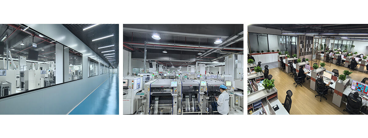
A.O.I
High-speed Automated Optical Inspection (AOI) for PCB/PCBA assemblies—detects soldering defects, component misplacement, and polarity errors with precision. IPC-A-610 compliant, non-destructive testing ensures consistent quality across prototyping and mass production runs.
✅ IPC-A-610 compliant testing
✅ Fast defect detection
✅ Non-destructive & high-speed inspection
✅ Reduces rework costs & production delays
Description
What is AOI?
AOI stands for Automated Optical Inspection, a critical quality control technology widely used in PCB and PCBA manufacturing processes. It uses high-resolution cameras, optical sensors, and machine vision algorithms to automatically detect defects on circuit boards without physical contact.
How AOI Works: The Inspection Process
Automated Optical Inspection (AOI) operates as a non-contact, vision-driven quality control system for PCB/PCBA manufacturing, relying on high-resolution imaging, intelligent algorithms, and reference comparison to detect surface defects. Its inspection process follows four core, sequential steps, ensuring precision and consistency across production lines.
Pre-Inspection Setup & Calibration
Before scanning boards, the AOI system requires configuration to match the specific PCB/PCBA design:
Load Reference Data: Import the CAD design file of the target board or use a golden sample—a verified defect-free board—as the inspection benchmark. The system maps key parameters: component positions, pad sizes, solder joint shapes, and trace layouts.
Optical Parameter Calibration: Adjust lighting conditions to highlight different defect types. For example, side lighting exposes solder joint height, while backlighting detects trace breaks. Calibrate camera focus and resolution to capture fine details of dense or miniaturized components.
Set Tolerance Thresholds: Define acceptable deviation ranges for component placement, solder volume, and polarity. This prevents false alarms while ensuring critical defects are flagged.
Image Acquisition
The AOI machine scans the PCB/PCBA surface to capture high-quality visual data:
The board is conveyed to the inspection area via an automated conveyor belt, ensuring stable positioning.
High-speed industrial cameras capture images of the board from multiple angles (2D or 3D, depending on the AOI model). 3D AOI uses laser scanning to measure height, enabling more accurate detection of solder joint volume and component coplanarity.
The system stitches individual images into a complete, high-resolution map of the entire board surface for full coverage inspection.
Image Analysis & Defect Detection
This is the core step where the system identifies anomalies through intelligent comparison:
· Pixel-by-Pixel Comparison: The captured board image is compared against the preloaded reference. The algorithm analyzes differences in pixel density, shape, position, and color.
· Defect Identification: Deviations beyond the preset tolerance thresholds are classified as potential defects. Common detected issues include:
· Component-related: Missing parts, polarity reversal, misalignment, or wrong component types.
· Solder-related: Solder bridges, insufficient solder, cold solder, or tombstoning.
· PCB-related: Trace scratches, missing pads, or silkscreen errors.
· 3D AOI Enhancement: 3D systems add height measurement analysis, distinguishing between acceptable solder fillets and defects like insufficient solder or excess solder that 2D AOI might miss.
Defect Reporting & Action
After analysis, the system generates actionable results for production teams:
· Defect Classification & Flagging: The AOI sorts defects by severity and marks their exact locations on the board map. Critical defects trigger immediate alerts.
· Data Logging & Reporting: Detailed inspection reports are stored, including defect types, locations, and occurrence rates. This data supports traceability and helps engineers identify recurring issues to optimize the SMT assembly process.
· Post-Inspection Handling: The board is either routed to a repair station for defect correction or passed to the next production stage if no defects are detected.
Key Application Stages in PCBA Production
AOI is deployed at multiple checkpoints to ensure full-process quality control:
· Pre-reflow AOI: Inspects component placement accuracy, polarity, and presence before soldering, preventing faulty components from entering the reflow oven.
· Post-reflow AOI: The most common application, checking solder joint quality and component integrity after reflow soldering.
· Post-assembly AOI: Performs a final inspection of the complete PCBA to ensure it meets design and industry standards before shipment.
What Does AOI Detect?
What Does AOI Check?
Automated Optical Inspection is a non-contact quality control tool for PCB/PCBA manufacturing, designed to detect surface-level defects by comparing board images against golden samples or CAD data. Its checks cover three core categories across different production stages:
PCB Substrate Defects
Before component assembly, AOI inspects the bare PCB for structural integrity:
· Trace defects: Scratches, breaks (open circuits), short circuits, or incorrect trace widths.
· Pad issues: Missing pads, misaligned pads, pad oxidation, or uneven pad surfaces.
· Surface flaws: Contamination, dust particles, solder mask peeling, or incorrect silkscreen printing (e.g., wrong component labels).
· Hole defects: Misaligned vias, missing holes, or oversized/undersized drilled holes.
Component Placement Defects
In the pre-reflow stage (after component mounting, before soldering), AOI verifies component accuracy:
· Presence/absence: Missing components or extra (unplanned) components on the board.
· Positioning errors: Misaligned components, offset placement, or rotation beyond tolerance.
· Polarity issues: Reversed component polarity.
· Incorrect components: Wrong part type, wrong value, or mismatched package size.
· Lead defects: Lifted leads, bent leads, or leads not properly seated on pads.
Solder Joint Defects
In the post-reflow stage (after soldering), AOI focuses on solder quality—the most common inspection target:
· Insufficient solder: Weak, incomplete joints that risk poor electrical contact.
· Excess solder: Bulky joints that may cause short circuits.
· Solder bridges: Unwanted solder connections between adjacent pads/traces.
· Cold solder: Dull, grainy joints with weak adhesion, caused by insufficient heating during reflow.
· Tombstoning: Component tilting (one end lifted off the pad) due to uneven solder melting.
· Solder balls: Tiny, stray solder particles that can lead to short circuits in dense PCBs.
Post-Assembly Final Checks
For fully assembled PCBA, AOI conducts a comprehensive final inspection:
· Overall assembly completeness and compliance with design specifications.
· Damage to components during soldering or handling.
· Conformance to industry standards for solder joint and component placement quality.
AOI’s checks are fast, consistent, and traceable—generating detailed defect reports to help manufacturers optimize production processes and reduce product failure rates.
| AOI Advantages | Manual Inspection Limitations | ||||
| High detection accuracy (up to micrometer-level precision) | Prone to human error and fatigue | ||||
| Fast inspection speed (handles hundreds of boards per hour) | Slow efficiency, unsuitable for mass production | ||||
| Consistent standards (no subjective judgment) | Results vary by inspector experience | ||||
| Non-contact measurement | Risk of physical damage during manual handling | ||||
| Data traceability (stores inspection records for process improvement) | Difficult to track and analyze defect trends |
Contrast
Types of AOI: 2D AOI vs. 3D AOI
In PCB/PCBA quality control, Automated Optical Inspection (AOI) is primarily divided into 2D AOI and 3D AOI based on imaging and measurement principles. Both technologies serve defect detection but differ significantly in accuracy, application scenarios, and core capabilities—especially for modern high-density, miniaturized circuit boards.
2D AOI
Core Principle: Uses 2D planar imaging technology, relying on high-resolution industrial cameras and multi-angle lighting to capture 2D images of PCB/PCBA surfaces. It detects defects by comparing the planar shape, size, and color of components, solder joints, and traces against reference CAD data or golden samples.
Key Features
· Advantages:
Low equipment cost and easy maintenance, suitable for small and medium-sized factories with basic inspection needs.
Fast scanning speed, ideal for high-volume production lines of standard PCBs.
Effective for detecting planar defects.
· Limitations:
Only captures surface planar information, unable to measure height and volume. It often misjudges or misses 3D-related defects.
Prone to false alarms due to lighting angle changes or component color variations.
Less effective for fine-pitch components and high-density PCBs.
· Typical Application Scenarios
Pre-reflow inspection of low-density PCBs (checking component presence, polarity, and placement offset).
Inspection of simple solder joint defects on consumer electronics PCBs.
Cost-sensitive production lines with basic quality requirements.
3D AOI
Core Principle: Combines 2D planar imaging with 3D height measurement technology (usually laser triangulation or structured light scanning). It projects laser or structured light onto the PCB/PCBA surface, calculates the 3D coordinates of each point by analyzing the light reflection angle and displacement, and constructs a complete 3D model of the board. Defect detection is based on both planar position and height/volume data.
Key Features
· Advantages:
Accurate measurement of solder joint height, volume, and component coplanarity—eliminating false alarms caused by 2D planar limitations. It can precisely identify defects like insufficient solder, excess solder, tombstoning, and lifted leads.
High detection accuracy for fine-pitch and complex components, which are common in automotive electronics, medical devices, and aerospace PCBs.
Supports quantitative analysis of defects, enabling data-driven process optimization.
· Limitations:
Higher equipment cost and longer scanning time compared to 2D AOI.
More complex calibration and maintenance, requiring professional technicians.
· Typical Application Scenarios
Post-reflow inspection of high-density, high-precision PCBs.
Inspection of complex solder joints (BGA, QFN) and miniaturized components.
Production lines with strict quality requirements.
| 2D AOI vs. 3D AOI: Head-to-Head Comparison | |||||
| Comparison Dimension | 2D AOI | 3D AOI | |||
| Imaging Principle | Planar 2D image capture | 2D imaging + 3D height measurement (laser/structured light) | |||
| Core Detection Capability | Planar defects (shape, position, color) | Planar defects + 3D defects (height, volume, coplanarity) | |||
| Accuracy for Fine-Pitch Components | Low (prone to false alarms/misses) | High (precise detection of micro-defects) | |||
| Equipment Cost | Low | High | |||
| Scanning Speed | Fast | Moderate (slower than 2D) | |||
| False Alarm Rate | High | Low | |||
| Typical Applications | Low-density, low-precision PCBs | High-density, high-reliability PCBs (automotive, medical, aerospace) | |||
Application
AOI in PCB and SMT: Key Application Scenarios
Automated Optical Inspection is an indispensable quality control tool throughout the PCB fabrication and SMT assembly processes. Deployed at critical production checkpoints, it ensures defect detection early, reduces rework costs, and maintains consistent product quality. Below are its core application scenarios, categorized by production stage.
AOI Applications in PCB Fabrication (Bare Board Inspection)
AOI is used to verify the structural integrity of bare PCBs before component mounting, targeting defects introduced during etching, drilling, and solder mask application.
Post-Etching Inspection
· Purpose: Check for trace defects that affect electrical connectivity.
· Detected Defects: Open circuits (broken traces), short circuits (unwanted trace connections), trace width deviations, under-etching/over-etching, and missing anti-pads.
· Value: Catches fatal electrical defects early, preventing costly rework after component assembly.
Post-Solder Mask & Silkscreen Inspection
· Purpose: Verify the accuracy of solder mask coverage and silkscreen printing.
· Detected Defects: Solder mask peeling, misaligned solder mask openings, solder mask bubbles, incorrect silkscreen labels, and silkscreen smudges.
· Value: Ensures solder mask protects traces from oxidation and silkscreen aids in subsequent component placement and troubleshooting.
Post-Drilling/Via Inspection
· Purpose: Inspect drilled holes and vias for mechanical accuracy.
· Detected Defects: Misaligned holes, oversized/undersized vias, plugged vias (unintended blockage), and missing vias.
· Value: Guarantees reliable interlayer connections in multi-layer PCBs.
AOI Applications in SMT Assembly Process
SMT is the core of PCBA production, and AOI is deployed at three key stages to cover component placement and soldering quality.
Pre-Reflow AOI
· Timing: After pick-and-place machines mount components, before the board enters the reflow oven.
· Purpose: Verify component placement accuracy before soldering—this is the most cost-effective checkpoint to fix defects.
Detected Defects:
Component issues: Missing components, extra components, wrong component type/value, reversed polarity.
Placement issues: Component offset, rotation beyond tolerance, lifted leads, and components not seated on pads.
Value: Avoids defective boards entering the reflow oven, reducing solder waste and rework labor.
Post-Reflow AOI
Timing: Immediately after the board exits the reflow oven (the most widely used AOI scenario in SMT).
Purpose: Inspect solder joint quality and post-soldering component integrity.
Detected Defects:
Solder joint defects: Solder bridges (short circuits between pads), insufficient solder, excess solder, cold solder (poor adhesion), tombstoning (component tilting), and solder balls.
Component damage: Cracked IC bodies, bent leads from high-temperature reflow, and displaced components.
Value: Ensures solder joints meet IPC standards and prevents reliability issues in end products.
Post-Assembly AOI
Timing: After manual insertion of through-hole components (if applicable) and functional testing.
Purpose: Conduct a comprehensive final check of the fully assembled PCBA.
Detected Defects: Missing through-hole components, incorrect hand-soldering, damaged connectors, and residual flux or contamination on the board surface.
Value: Serves as the final quality gate before shipment, ensuring only qualified products reach customers.
Specialized Application Scenarios for High-Reliability Industries
For industries with strict quality requirements, AOI is tailored to specific needs:
· Automotive Electronics: 3D AOI is used to inspect PCBA for engine control units (ECUs) and ADAS systems, focusing on solder joint coplanarity and component reliability under high-temperature conditions.
· Medical Devices: AOI verifies PCBA for pacemakers, diagnostic equipment, etc., ensuring zero defects to comply with FDA and ISO 13485 standards.
· Aerospace & Defense: High-precision 3D AOI inspects miniaturized, high-density PCBA for avionics, detecting micro-defects that could cause system failure in extreme environments.