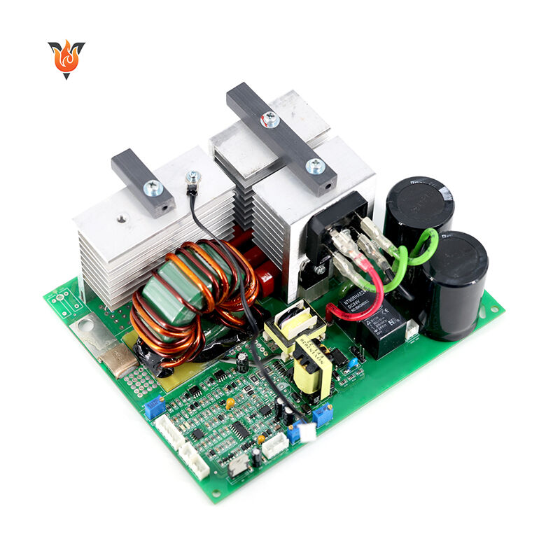
Design Rule Check
Professional Design Rule Check services for PCB designs—avoid manufacturing errors, ensure compliance, and boost efficiency. Our expert team validates layouts against industry standards, fabrication constraints, and signal integrity requirements, minimizing rework and accelerating time-to-market.
Tailored for medical, industrial, automotive & consumer electronics, we offer fast turnaround, detailed error reports, and DFM-aligned checks. Trust our DRC support to turn your PCB designs into production-ready files with zero costly flaws.
Description
Design Rule Check
Design rule check, more commonly called as DRC in the PCB industry, is a physical design process to determine if the physical layout satisfies a number of rules or recommended parameters defined by the semiconductor manufacturers. DRC also involves LVS(layout and schematic)inspection, XOR inspection, ERC (electrical rule inspection), and antenna inspection.
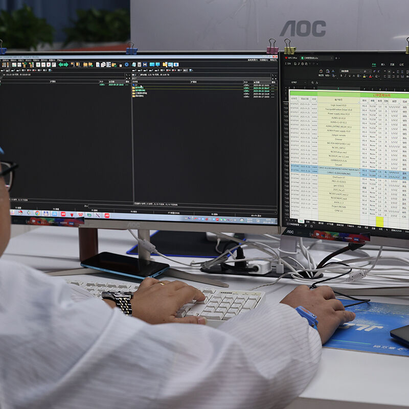
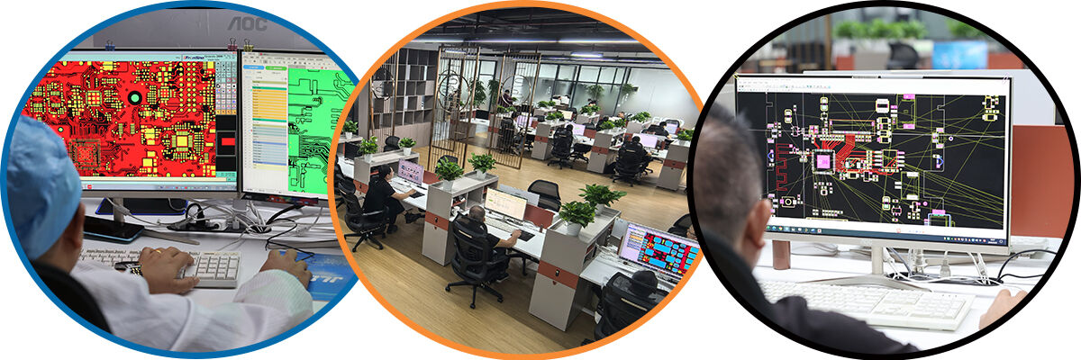
PCB design and manufacturing is a highly complex process requiring the effective management of thousands of components and connections on multi-layered boards. Ensuring production yield is crucial, and Design Rule Check is a key method for improving it. DRC is a critical verification step in the PCB design process, using EDA tools to automatically check whether the PCB layout conforms to preset design rules and manufacturing constraints, ensuring the design is manufacturable and reliable.
These rules typically include:
• Electrical rules: such as minimum trace width, trace spacing, and pad and trace connection specifications to avoid short circuits or signal interference;
• Manufacturing rules: such as minimum hole diameter, via width, and solder mask (solder mask) opening size to match the PCB factory's processing capabilities;
• Process rules: such as component spacing and positioning reference point settings to meet the precision requirements of SMT assembly equipment. The core function of DRC is to detect potential design errors and violations, reducing rework in later production, lowering costs, and shortening the development cycle.
The core value and importance of Design Rule Check (DRC) in PCBA manufacturing
Design Rule Check is a critical quality control step in the entire PCBA process from design to mass production. By setting industry standards, manufacturing process constraints, and reliability requirements, it automates or manually verifies PCB design documents. Its importance spans the entire chain of design verification, cost control, mass production assurance, and quality improvement. It is a core pre-process for Kingfield to ensure the competitiveness of its PCBA products.
I. Avoid design flaws and reduce mass production risks
DRC can accurately identify hidden problems in the design, including non-compliant trace width/spacing, abnormal via dimensions, mismatch between pads and device packages, poor copper connections, and power and ground network layout conflicts. If these issues are not identified during the design phase, they can lead to fatal failures such as PCB short circuits/open circuits, inability to solder components, and signal interference during prototyping or mass production. This not only wastes raw materials but also delays project delivery. Kingfield uses a rigorous DRC process to intercept design defects early, controlling risks at the source and ensuring that the design meets manufacturing feasibility requirements.
II. Matching manufacturing processes to ensure production efficiency
Different PCBA manufacturers have varying production equipment and process capabilities. DRC can customize inspection rules based on Kingfield's core process parameters to ensure a high degree of matching between design documents and actual production capabilities. For example, for micro-via designs on high-density PCBs, DRC can verify whether the hole diameter meets the drilling equipment precision, avoiding production interruptions and yield reductions due to process incompatibility. DRC achieves seamless integration of "design-manufacturing," significantly improving production efficiency and shortening delivery cycles.
III. Control cost losses and optimize resource allocation
Design flaws leading to rework/remanufacturing are one of the main reasons for cost overruns in PCBA projects. For example, if a PCB short circuit occurs due to excessively close trace spacing, the circuit board needs to be remade, components repurchased, and secondary processing required, directly increasing material and labor costs. If problems are discovered after mass production, the losses will be exponentially amplified. Kingfield uses DRC to identify problems in advance, minimizing rework rates and avoiding material waste due to unreasonable design, achieving precise cost control and improving project profitability.
IV. Ensure product reliability and enhance brand reputation
The reliability of PCBA products directly depends on the rationality of their design. DRC can verify the design scheme from multiple dimensions, including electrical performance, mechanical structure, and thermal stability:
Electrical performance: Verify the rationality of power network voltage drop, signal impedance matching, and grounding design to avoid product malfunctions caused by signal interference or power instability;
Mechanical structure: Check whether the component layout meets heat dissipation requirements and whether connectors have sufficient insertion and removal space to avoid affecting product lifespan due to heat accumulation or mechanical interference;
Environmental adaptability: For special scenarios such as industrial and automotive applications, DRC can verify whether the design meets environmental standards such as vibration resistance and high temperature resistance. DRC ensures stable operation of products throughout their entire lifecycle, reduces after-sales maintenance costs, and strengthens Kingfield's brand reputation and market competitiveness in the PCBA industry.
V. Adapt to industry standards and meet compliance requirements
PCBA products for different applications must comply with relevant industry standards. DRC can embed the mandatory requirements of these standards to ensure product compliance certification. For example, in automotive electronics PCBA design, DRC can verify the isolation distance between high-voltage and low-voltage circuits to meet automotive electronic safety standards; in medical device PCBAs, it can check signal integrity design to ensure the accuracy of device diagnostics. Kingfield ensures product compliance with industry standards through DRC, providing customers with compliant and reliable customized solutions.
DRC is a core function in PCBA
Design Rule Check, as a core tool for PCBA design verification, performs comprehensive and detailed checks on PCB design documents through a standardized rule base and intelligent verification logic. Its functions cover key dimensions such as electrical performance, manufacturing feasibility, mechanical structure, and compliance, and it is a core technological support for Kingfield to ensure PCBA design quality and mass production reliability. The following details its eight core functions:
I. Electrical Rule Verification: Ensuring Stable Circuit Function
Electrical performance is the core of PCBA products. DRC precisely verifies the electrical rationality of circuit design to avoid problems such as signal abnormalities and power instability from the source:
• Spacing rule check: Verifies the minimum insulation spacing between conductors, pads, vias, and copper traces to avoid short circuits and creepage caused by insufficient spacing, especially suitable for the stringent requirements of high-voltage circuits and high-density PCBs;
• Network connectivity verification: Detects network problems such as open circuits, short circuits, and loose connections to ensure that the connectivity of power, signal, and ground networks meets design specifications, avoiding functional failures due to network breaks;
• Impedance matching verification: For high-speed signals, checks whether the transmission line width, line spacing, and dielectric thickness meet the preset impedance values to reduce signal reflection and crosstalk, ensuring signal integrity;
• Power network verification: Verifies whether the power rail width meets the current carrying capacity requirements (avoiding overload heating) and whether the power and ground distribution is balanced (reducing voltage drop), ensuring stable power supply;
• Grounding design inspection: Check whether the grounding method (single-point grounding, multi-point grounding) is reasonable and whether the number of grounding vias is sufficient to avoid ground loop interference and improve the circuit's anti-interference capability.
II. Manufacturing process compatibility check: Ensure production feasibility
DRC customizes rules based on Kingfield's production equipment parameters and process capabilities to ensure seamless compatibility between the design and the actual manufacturing process:
• Line width/spacing check: Verify that the conductor width meets the minimum processing requirements, avoiding etching breakage and insufficient current carrying capacity due to excessively thin line width;
• Via parameter verification: Check that the via diameter, wall thickness, and pad size match the drilling and copper plating processes, avoiding via blockage and poor connection;
• Pad design verification: Confirm that the pad size and spacing are consistent with the device package, avoiding oversized/undersized pads that cause cold solder joints and solder bridges, and ensuring compatibility with SMT mounting and reflow soldering processes;
• Solder mask/silk screen check: Check whether the solder mask opening covers the pad and whether the silk screen overlaps, ensuring accurate device positioning during production;
• Copper processing verification: Check the connection method between the copper and the pads and vias, copper islands, and adapt to PCB etching and solder mask process requirements.
III. Mechanical Structure and Thermal Design Inspection: Improving Product Reliability
DRC optimizes the design from the perspective of physical structure and thermal stability, ensuring the mechanical strength and heat dissipation capacity of the PCBA throughout its entire life cycle:
• Component layout verification: Checks whether the component spacing meets heat dissipation requirements and whether there is mechanical interference, reserving sufficient assembly and heat dissipation space;
• Board edge distance check: Verifies the minimum distance from components, vias, copper traces to the PCB edge, avoiding circuit damage and insufficient mechanical strength caused by board edge cutting;
• Heat dissipation design verification: For high-power components, checks whether the design of heat dissipation pads and heat dissipation vias is reasonable, ensuring rapid heat conduction and avoiding heat accumulation leading to component aging;
• Mechanical hole verification: Checks whether the size and position of screw holes and positioning holes match the housing and mounting structure, avoiding assembly failure due to hole deviations.
IV. Device and Package Compatibility Check: Mitigating Assembly Risks
Design Compatibility Check verifies the consistency between device packages and design documents to avoid assembly problems caused by package errors:
• Package Matching Check: Confirms that the device package matches the actual selected device, avoiding "package-device mismatch" that prevents soldering;
• Polarity Component Verification: Checks whether the package polarity of polarized components such as diodes, capacitors, and integrated circuits matches the design logic, avoiding reverse soldering that could burn out the device;
• Component Placeholder Check: Investigates unspecified packages and duplicated components, ensuring that the component information in the BOM (Bill of Materials) completely matches the component information in the design documents.
V. Special Inspection for High-Density and Special Processes: Adapting to Complex Designs
For PCBs with special processes such as HDI, rigid-flex PCBs, and buried/blind vias, DRC offers customized specialized inspection functions:
• HDI Process Inspection: Verifies whether the via diameter, position accuracy, and stacking structure meet HDI process requirements to prevent via interconnect failures;
• Buried/Blind Via Verification: Checks the conductivity of buried/blind vias and their connection to outer layer circuits to ensure stable interlayer signal transmission;
• Rigid-Flex PCB Inspection: Verifies whether the transition design between flexible and rigid areas and the bending radius meet the requirements of flexible PCB processes to prevent circuit breakage during bending.
VI. Compliance and Industry Standards Inspection: Meeting Scenario-Specific Requirements
DRC incorporates mandatory standards from various industries to ensure PCBA products meet the compliance requirements of their application scenarios: Electromagnetic Compatibility (EMC) checks: Verify whether the layout of filter capacitors, ground plane integrity, and signal shielding design comply with EMC standards to reduce electromagnetic radiation and interference; Industry-specific standard verification:
• Automotive electronics: Complies with IATF 16949 standards, checking the isolation distance between high-voltage and low-voltage circuits and vibration resistance design;
• Medical equipment: Complies with ISO 13485 standards, verifying signal integrity and insulation design to ensure accurate equipment diagnostics;
• Industrial control: Checks anti-interference and wide-temperature adaptability design to meet the stability requirements of industrial environments;
• Safety compliance checks: For mains-powered PCBAs, verify whether creepage distances and clearances comply with safety standards such as IEC 60950 to avoid the risk of electric shock.
VII. Design Optimization Suggestion Function: Improve Design Efficiency
Advanced DRC tools not only "find problems" but also provide intelligent optimization suggestions to help engineers quickly iterate designs:
• Automatic problem location marking: Precisely mark violation locations through a visual interface, supporting one-click jump to the corresponding area in the design file;
• Optimization solution recommendations: Provide specific solutions for violations, such as "insufficient line width, suggest adjusting to 0.15mm" or "pad spacing too small, suggest increasing to 0.3mm";
• Batch repair function: Support batch automatic repair of recurring simple violations, significantly improving design modification efficiency.

