1. مقدمه: اهمیت بهینهسازی یکپارچگی سیگنال در طراحی PCB چندلایه ترکیبی
در چشمانداز الکترونیک امروز که به سرعت در حال تحول است، تقاضا برای دستگاههای کوچک و با عملکرد بالا منجر به ادغام مدارهای آنالوگ و دیجیتال روی یک pCB ترکیبی شده است. این بردها همه چیز را از کنترلکنندههای صنعتی هوشمند تا سیستمهای سرگرمی-اطلاعاتی خودرو تغذیه میکنند و در مرکز عملکرد آنها یک جنبه حیاتی قرار دارد: سلامت سیگنال .
یکپارچگی سیگنال (SI) به کیفیت و قابلیت اطمینان سیگنالهای الکتریکی در عبور از یک برد مدار چاپی اشاره دارد. وقتی سیگنالی شکل، ولتاژ و زمانبندی مورد نظر خود را در طول حرکت حفظ کند، سیستم مطابق انتظار عمل میکند. با این حال، با وجود بخشهای دیجیتال با سرعت بالا در pCB دیجیتال و مدارهای حساس آ نالوگ PCB در صورت همزیستی دامنههای مختلف در چیدمان سیگنال ترکیبی، تهدیدهای مربوط به کیفیت سیگنال افزایش مییابد. انتقالهای با فرکانس بالا، نویز سوئیچینگ و اثرات پارازیتی میتوانند سیگنالها را تضعیف کنند و منجر به crossTalk , جهش زمین ، و از دست دادن وفاداری داده شوند. پیامدها چیست؟ رفتار غیرقابل پیشبینی مدار، تداخل الکترومغناطیسی ( EMI )، مشکلات نظارتی و تأخیرهای طولانی در رسیدن به بازار.
چرا یکپارچگی سیگنال در بردهای مدار چاپی سیگنال ترکیبی اهمیت بالایی دارد؟
بردهای سیگنال ترکیبی با چالشهای خاصی در یکپارچگی سیگنال (SI) مواجه هستند، زیرا مدارهای دیجیتالی نرخ لبههای سریع، نوسانات ولتاژ و جریانهای ناگهانی تولید میکنند که به راحتی میتوانند مسیرهای آنالوگ را آلوده کنند. یک نوک ناخواسته روی یک ولتاژ مرجع صفحه زمین یا یک کلاک خراب میتواند به معنای قرائتهای نادقیق آنالوگ، شکست در یکپارچهسازی ADC ، یا انتقال دادههای خراب باشد—که همه این موارد بهویژه در کاربردهای حساس از نظر ایمنی یا با وضوح بالا بسیار جدی هستند.
جدول حقایق سریع: چرا یکپارچگی سیگنال در بردهای مدار چاپی سیگنال ترکیبی مهم است
|
مشکل
|
اثر دیجیتال برد مدار چاپی
|
اثر آنالوگ برد مدار چاپی
|
تأثیر در دنیای واقعی
|
|
CrossTalk
|
خطاهای بیتی
|
왜곡된 سیگنال
|
خروجی نامطمئن، نویز سیستم
|
|
جهش زمین
|
خرابی زمانبندی
|
تغییرات مرجع
|
لبههای از دست رفته، دقت نادرست ADC
|
|
مدیریت EMI / EMC
|
عدم موفقیت در انتشارات
|
افزایش سر و صدا
|
عدم تطابق با گواهینامههای نظارتی
|
|
حلقههای مسیر بازگشت
|
انحراف، لرزش
|
غرش، جمعآوری نویز
|
سنسوردهی نادرست، برق ضعیف
|
سرفصلهای این راهنما
در این راهنمای تفصیلی، شما خواهید آموخت:
- مبانی pCB ترکیبی مهندسی
- بهترین روشهای عملی برای مدیریت SI (با کلمات کلیدی مانند امپدانس کنترلشده , مسیریابی جفت دیفرانسیلی ، و استراتژیهای ارتینگ )
- فرآیند ۱۲ مرحلهای برای بیشینهسازی عملکرد و قابلیت ساخت
- پوشش پیشرفته ویاس، استکآپها، خازنهای رفع نویز و موارد بیشتر
- راهنماییهای عیبیابی و مثالهای موردی
- آخرین ابزارها برای شبیهسازی SI و تحلیل PDN
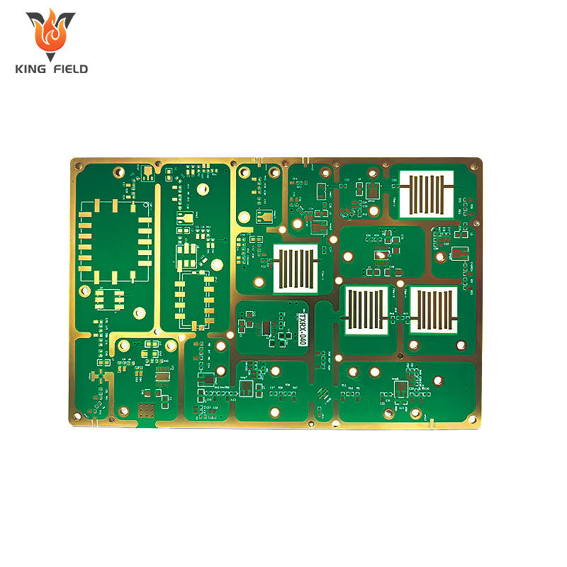
۲. طراحی برد الکترونیکی ترکیبی آنالوگ و دیجیتال چیست؟
آمپر pCB ترکیبی یک برد مدار چاپی است که مؤلفههای آنالوگ و دیجیتال را در یک زیرساخت واحد ادغام میکند. این ادغام به دستگاههای مدرن اجازه میدهد تا جهان فیزیکی —آنالوگ— را با حوزه دیجیتال پیوند دهند و همه چیز را از محصولات اینترنت اشیا غنی از سنسور تا واحدهای کنترل الکترونیکی پیشرفته خودروها ممکن میسازند.
تعریف حوزههای برد الکترونیکی ترکیبی، آنالوگ و دیجیتال
- مدارهای آنالوگ PCB سیگنالهای پیوسته مانند صدا، دما یا سطح ولتاژ را پردازش میکنند. این سیگنالها بسیار حساس به نویز، تداخل و نوسانات کوچک ولتاژ هستند.
- مدارهای دیجیتال PCB سیگنالهای منطقی گسسته (0 و 1) را پردازش میکنند. هرچند که ممکن است مقاوم به نظر برسند، اما مدارهای دیجیتال — به ویژه مدارهای با سرعت بالا — منابع عمدهای از نویز الکترومغناطیسی، نوسان زمین (ground bounce) و خروجیهای همزمان تعویض شونده (SSO) هستند.
- طراحی مدارهای PCB ترکیبی (mixed-signal) به چیدمانهایی اطلاق میشود که در آن این دو دنیا باید در کنار هم عمل کنند و نیازمند توجه فراوان به سلامت سیگنال ، زمینبندی و مسائل مربوط به یکپارچگی تغذیه هستند.
کاربردهای متداول مدارهای PCB ترکیبی
مدارهای PCB ترکیبی ستون فقرات بسیاری از سیستمهای حیاتی هستند، از جمله:
- اتوماسیون صنعتی: کنترل بلادرنگ با رابطهای حسگر با دقت بالا.
- سیستمهای خودرویی: اطلاعرسانی و سرگرمی، مدیریت باتری، سیستمهای کمک رانندگی پیشرفته و کنترل موتور.
- لوازم الکترونیکی مصرفی: تلفنهای همراه هوشمند، دستگاههای قابل پوشیدن، تجهیزات صوتی و دوربینها.
- تجهیزات پزشکی: مانیتورهای بیمار، سیستمهای تصویربرداری و تجهیزات تشخیصی.
- ارتباطات: روترها، فرستنده-گیرندهها، SDR و تجهیزات شبکه با سرعت بالا.
جدول: نمونه موارد استفاده از برد مختلط سیگنال
|
کاربرد
|
دستگاه نمونه
|
بخش آنالوگ
|
بخش دیجیتال
|
|
کنترل صنعتی
|
کنترلکننده PLC
|
ورودی سنسور ترموکوپل
|
میکروکنترلر و PHY اترنت
|
|
خودرویی
|
سیستم مدیریت باتری
|
سنجش ولتاژ سلول
|
ماژول کنترل بار باتری
|
|
پزشکی
|
دستگاه الکتروکاردیوگرام قابل حمل
|
پیشامواج سیگنال بیمار
|
میکروکنترلر بیسیم بلوتوث
|
|
مصرفکننده
|
بلندگوی هوشمند
|
کدک صوتی و میکروفون
|
وایفای/بلوتوث، پردازش سیگنال دیجیتال
|
|
ارتباطات
|
رادیوی SDR
|
پیشامواج فرکانس رادیویی و فیلتر کردن فرکانس میانی
|
FPGA، DSP، اترنت
|
چرا طراحی برد مدار چاپی ترکیبی سیگنال دشوار است؟
چالش اصلی، مدیریت سلامت سیگنال است، زیرا:
- مدارهای دیجیتالی تغییرات ولتاژ سریعی ایجاد میکنند (dV/dt بالا، di/dt بالا) که نویز القا میکنند در زمینهای مشترک و شبکههای تغذیه.
- مدارهای آنالوگ در برابر نویزهای سطح پایین حساس هستند، حتی در سطوح میکروولتی، که میتواند باعث SNR کاهش نسبت سیگنال به نویز (SNR) و THD افزایش اعوجاج هارمونیکی کل (THD) در مبدلهای آنالوگ به دیجیتال (ADC) شود.
- سیگنالهای کلاک (مانند آنهایی که به یکپارچهسازی ADC ) و خطوط داده از چندین حوزه عبور میکنند که منجر به crossTalk , ناپیوستگیهای مسیر بازگشت ، و خطاهای زمانبندی میشود.
- اجرا نامناسب استراتژیهای ارتینگ و PCB stack-up میتواند این خطرات را تشدید کند، بهویژه در بوردهای چندلایه متراکم.
درک بلوکهای اصلی سیگنال ترکیبی
یک برد الکترونیکی موفق با سیگنال ترکیبی به موارد زیر دست مییابد:
- جدا کردن: نگهداری سیگنالهای آنالوگ بدون نویز دیجیتال از طریق چیدمان مناسب، تقسیم زمین یا حلقههای محافظ.
- تبدیل قابل اعتماد: اطمینان از دقت و دادههای کم-جیتر در مبدلهای آنالوگ به دیجیتال (ADC) شما (مثلاً 12 بیتی یا 16 بیتی) و مبدلهای دیجیتال به آنالوگ (DAC) با استفاده از توزیع پالس ساعت شبکههای تمیز و مدارهای رگولاسیون بهینهشده.
- امپدانس کنترلشده: رعایت خطوط 50 اهم تکسر (single-ended) یا 100 اهم دیفرانسیلی برای ردیابهای نرخ داده بالا با استفاده از ساختارهای میکرواستریپ، استریپلاین یا موجبر همصفحه.
- شبکه تحویل توان مؤثر (PDN): کاهش افت ولتاژ و حفظ ولتاژهای پایدار با استفاده از خازنهای رگولاسیون مناسب و طراحی صفحه توان.
- سپرزنی و مدیریت EMI: استفاده از via stitching، پرش مسی یا قفس فارادی در مناطق حساس کلیدی.
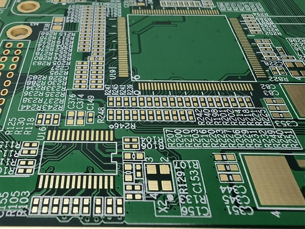
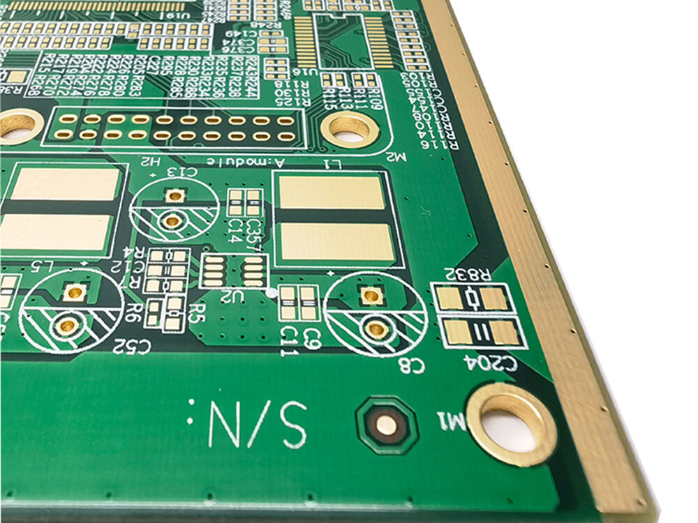
3. چالشهای کلیدی یکپارچگی سیگنال در برد الکترونیکی ترکیبی آنالوگ و دیجیتال
طراحی یک سیستم قوی pCB ترکیبی عملی حساس است که نیازمند هماهنگی دقیق بین حساسیت آنالوگ و فعالیت پیوسته منطق دیجیتال روی یک زیرساخت مشترک است. با افزایش نرخ دادهها و تراکم بیشتر در برد، تضمین یکپارچگی سیگنال (SI) دیگر تنها چالشبرانگیز نیست، بلکه ضروری میشود. در ادامه، مهمترین موانع یکپارچگی سیگنال را بررسی میکنیم که هر طراح برد الکترونیکی ترکیبی باید برای تحویل محصولات قابل اعتماد و با عملکرد بالا به آنها رسیدگی کند. سلامت سیگنال (SI) شدن یکپارچگی سیگنال
1. تداخل سیگنال و انتقال نویز
هرگاه ردیفهای آنالوگ و دیجیتال به صورت نزدیک به یکدیگر قرار گیرند، به ویژه در طول بازههای موازی بلند، سیگنالهای دیجیتالی با تغییر سریع، نویز را از طریق خازن متقابل و القای متقابل به خطوط حساس آنالوگ منتقل میکنند — پدیدهای که به آن crossTalk تداخل سیگنال (Crosstalk) گفته میشود. در طراحیهای با سرعت بالا، این موضوع میتواند خطاهای قابل توجهی در اندازهگیریهای آنالوگ ایجاد کند یا دادهها را خراب کند. زمینهای نامناسب مسیریابی جفت دیفرانسیلی و امپدانسهای بدون تطابق این مشکل را تشدید میکنند.
2. جهش ولتاژ زمین و حلقههای زمین
جهش زمین هنگامی رخ میدهد که خروجیهای دیجیتال با سرعت بالا به طور همزمان تغییر وضعیت دهند و باعث جابجایی ناگهانی ولتاژ زمین شوند. این تغییرات (خروجیهای سوئیچینگ همزمان، یا SSO) به ویژه در مواردی که بخش آنالوگ و دیجیتال تمام یا بخشی از صفحه زمین را به اشتراک میگذارند، مشکلساز است. این امر نه تنها منجر به خطاهای زمانبندی دیجیتال میشود، بلکه ولتاژهای مرجع برای تبدیلکنندههای آنالوگ به دیجیتال، تقویتکنندههای عملیاتی و حسگرهای حساس را نیز مختل میکند.
حلقههای زمین هنگامی رخ میدهند که چندین مسیر بازگشت زمین وجود داشته باشد و حلقههای ناخواستهای تشکیل شود که مانند «آنتن» عمل کرده و موجب ایجاد سر و صدا، نوسان یا دریافت EMI محیطی میشوند. این موضوع باعث میشود استراتژیهای ارتینگ —مانند طراحی دقیق چیدمان و اتصال زمین در یک نقطه— برای بردهای سیگنال ترکیبی بسیار حیاتی باشد.
3. نویز شبکه توزیع توان (PDN)
ناپایداریهای روی خطوط تغذیه، که توسط بارهای سریع سوئیچینگ (ICهای دیجیتال، درایورهای کلاک) ایجاد میشوند، میتوانند باعث ایجاد امواج نوسانی و پالسهای نویز شوند که مستقیماً به خطوط تغذیه آنالوگ یا ورودیهای مرجع آنالوگ القا میشوند. اگر خازنهای فیلتر اگر به میزان کافی نباشند، در جای اشتباه قرار گرفته باشند یا ویژگیهای ESR ضعیفی داشته باشند، کیفیت توان آسیب میبیند. یک PDN نه تنها SI را تضعیف میکند، بلکه دقت ADC را نیز به خطر میاندازد (که منجر به جیتر، کاهش نسبت سیگنال به نویز و حتی خطاهای عملکردی میشود).
۴. ناپیوستگیهای امپدانس و اختلال در مسیر بازگشت
سیگنالهای دیجیتال با سرعت بالا مانند خطوط انتقال با امپدانس کنترلشده عمل میکنند (معمولاً مایکرواستریپ یا استریپلاین)، و هرگونه ناپیوستگی — مانند یک ویا، کانکتور یا صفحه برق/زمین تقسیمشده که بهدرستی طراحی نشده باشد — باعث انعکاس سیگنال، امواج ایستاده و عدم تطابق امپدانس میشود. به همین ترتیب، مسیرهای بازگشت برای سیگنالهای آنالوگ و دیجیتال باید کوتاه، مستقیم و عاری از شکاف یا دندانه باشند، در غیر این صورت انعکاسها و کاهش سیگنال روی داد.
جدول: رایجترین اختلالات و اثرات آنها
|
نوع اختلال
|
نوع سیگنال
|
تأثیر معمول
|
|
تقسیم صفحه زمین
|
دیجیتال/ساعت
|
چولگی، نویز الکترومغناطیسی، خطاهای زمانبندی
|
|
محل اتصال مدار باقیمانده (ویا استاب)
|
دادههای پرسرعت
|
نوسان، جیتر بیش از حد، انعکاسها
|
|
برش صفحه برق
|
آنالوگ
|
همهمه، افت ولتاژ منبع تغذیه
|
|
منطقه تداخل سیگنال
|
آنتیاخطار/دیجیتال
|
خرابی دادهها، نویز و تغییرات جابهجایی
|
5. چالشهای EMI/EMC
اختلال الکترومغناطیسی (EMI) و سازگاری الکترومغناطیسی (EMC) چالشهای گستردهای هستند، بهویژه در طرحهای مدارهای ترکیبی سیگنال. مدارهای دیجیتال با لبههای سریع به عنوان فرستندههای EMI عمل میکنند، در حالی که سنسورهای آنالوگ، ورودیهای RF و ADCها «دریافتکنندههای» آسیبپذیر هستند. عدم کفایت پوشش دادن طرحبندی ضعیف صفحه و عدم استفاده از via stitching میتواند تبدیل به یک آنتن پخش زمینی شود و باعث عدم گذراندن گواهیهای نظارتی شود.
6. مشکلات زمانبندی سیگنال و توزیع کلاک
نامنظم شبکههای تمیز یا بیشازحد جیتر کلاک میتواند باعث عدم هماهنگی زمانی (skew) بین دامنهها شود و منجر به تأخیر غیرقابل پیشبینی، حالت متاستابل و خطاهای نمونهبرداری داده شود — بهویژه در هنگام عبور از دامنه کلاک . مبدلهای آنالوگ به دیجیتال و دیجیتال به آنالوگ بهویژه در برابر نویز و جیتر کلاک آسیبپذیر هستند که این امر باعث کاهش پهنای باند مؤثر و دقت میشود.
7. شبیهسازی ناکافی و تحلیل قبل از چیدمان
پیچیدگی مدرن برد مدار چاپی (PCB) باعث میشود که بدون استفاده از شبیهسازی SI و یکپارچگی توان (PI) تحلیل، خطرناک باشد. ابزارهای شبیهسازی (مانند HyperLynx، Ansys SIwave، Keysight ADS) به مهندس طراح اجازه میدهند تا مشکلات ظریفی مانند عدم تطابق طول، ناپیوستگی مسیر بازگشت، خازن فرعی و نقاط داغ حرارتی را خیلی پیش از تولید پیشبینی و اصلاح کند.
4. بهترین شیوهها و ملاحظات کلیدی
طراحی یک pCB ترکیبی با خواص استثنایی سلامت سیگنال نیازمند رویکردی ظریف و جامع است. هر تصمیم — از ترتیب لایهها تا توزیع توان — میتواند بر عملکرد نهایی برد در کاربردهای واقعی تأثیر بگذارد. در این بخش، شما با شیوههای اساسی و قابل اجرا آشنا میشوید که هم اصول بنیادی طراحی و هم تکنیکهای پیشرفته ادغام آنالوگ/دیجیتال را پوشش میدهند.
1. در ابتدا تقسیمبندی برد را برنامهریزی کنید
جداسازی عملکردی واضح بسیار مهم است. مناطق اختصاصی را برای آ نالوگ PCB و pCB دیجیتال مدارها در طول ثبت نمودار و برنامهریزی طرح کف. فاصله فیزیکی بهطور قابل توجهی از اتصال نویز، نوسان زمین و تداخل بین دامنهها میکاهد. یک اصل کلی: هرگز سیگنالهای ساعت دیجیتال یا دادههای پرسرعت را زیر یا در نزدیکی مؤلفههای آنالوگ حساس عبور ندهید.
اقدامات کلیدی:
- ADC، سنسورها و تقویتکنندههای آنالوگ را تا حد امکان دور از نوسانسازها، FPGAها، منابع تنظیمکننده سوئیچینگ و منابع کریستالی با فرکانس بالا قرار دهید.
- اتصالات اصلی دادههای دیجیتال را به گونهای جهتدهی کنید که نسبت به مسیرهای سیگنال آنالوگ حیاتی عمود باشند تا اتصال خازنی محدود شود.
2. بهینهسازی استقرار PCB شما
PCB stack-up بر همه چیز از مقاومت در برابر EMI تا کنترل امپدانس تأثیر میگذارد. از ساختار لایهای استفاده کنید که لایههای سیگنال پرسرعت را بین صفحات زمین جامد (و در صورت نیاز، صفحات تغذیه) بدون شکاف قرار دهد. این کار نه تنها خطوط انتقال امپدانس کنترلشده ایجاد میکند، بلکه مسیرهای بازگشتی کوتاه و مستقیم برای جریانهای گذرا سریع را فراهم میکند.
|
مثال استقرار لایهها
|
لایه
|
عملکرد
|
|
1 (بالا)
|
سیگنال
|
سیگنالهای دیجیتال/آنالوگ با سرعت بالا
|
|
2
|
صفحه زمین
|
مسیر بازگشت سیگنال اصلی (GND)
|
|
3
|
صفحه برق
|
منبع تغذیه آنالوگ/دیجیتال کمنویز (VCC)
|
|
4 (پایین)
|
سیگنال / GND
|
سیگنالهای با سرعت پایین، جزایر زمین محلی
|
3. استراتژیهای اصلی زمینکردن
زمینکردن سنگ بنای یکپارچگی سیگنال در مدارهای ترکیبی است. به طور کلی دو دیدگاه اصلی وجود دارد:
- زمین تکنقطهای (ستارهای): یک اتصال اختصاصی بهصورت کنترلشده ای بین بازگشت سیگنالهای آنالوگ و دیجیتال برقرار میکند—که بهویژه در طراحیهای با فرکانس پایین و متوسط بسیار مؤثر است.
- صفحه زمین پیوسته: برای طراحیهای با سرعت و فرکانس بالا، یک صفحه مسی جامد و پیوسته با تقسیمبندی دقیق (در صورت نیاز) کوتاهترین مسیرهای بازگشت را فراهم کرده و کمترین تولید EMI را دارد.
بهترین تکنیکهای زمینکردن برای برد های ترکیبی سیگنال:
- حلقههای زمین را اجتناب کنید با اطمینان از وجود تنها یک مسیر بازگشتی برای هر عملکرد مداری.
- صفحات زمین را بهصورت دلخواه تقسیم نکنید. فقط در صورت ضرورت کامل آنها را تقسیم کنید و همیشه در یک نقطه واحد با امپدانس پایین زیر ADC یا مبدل اصلی به هم متصل کنید.
- از حلقههای محافظ یا ریختهای مسی در اطراف خطوط آنالوگ با امپدانس بالا و مدارهای آنالوگ حساس استفاده کنید تا آنها را بیشتر محافظت نمایید.
4. کنترل امپدانس و استفاده از مسیریابی جفت دیفرانسیلی
ردیفهای دیجیتال با سرعت بالا باید به صورت امپدانس کنترلشده خطوط، متناسب با الزامات رابط (50 Ω تکسر، 100 Ω دیفرانسیلی معمول) مسیریابی شوند. این امر بازتاب سیگنال و امواج ایستاده را به حداقل میرساند. برای سیگنالدهی دیفرانسیلی (اترنت، LVDS، USB، HDMI)، فاصلهگذاری و تطبیق طول ردیفها ضروری است.
5. توزیع قوی و جداسازی مناسب توان را تضمین کنید
شما شبکه توزیع توان (PDN) نیازمند مهندسی جدی است.
- از منظمکنندههای جداگانه یا دامنههای فیلترشده برای ریلهای آنالوگ و دیجیتال استفاده کنید. از منظمکنندههای خطی کمنویز (LDO) برای بخش آنالوگ و منظمکنندههای سوئیچینگ (SMPS) برای بارهای دیجیتال استفاده کنید و در صورت نیاز فیلتر کنید.
- خازنهای جداساز (دکوپلینگ) را به صورت استراتژیک (شامل مقادیر متعدد برای فیلتر کردن فرکانسهای پایین و بالا) در نزدیکترین فاصله ممکن به پینهای تغذیه IC قرار دهید. خازنهایی با ESR پایین انتخاب کنید و از ترکیب خازنهای سرامیکی MLCC (0.01 μF، 0.1 μF، 1 μF و غیره) استفاده کنید.
- از دانههای فریت استفاده کنید یا سیمپیچهای کوچک جداساز بین صفحات/ریلهای آنالوگ و دیجیتال قرار دهید.
جدول نمونه جداکننده
|
ریل
|
نوع سرپوش
|
مقدار (معمول)
|
قرارگاه
|
|
دیجیتال 3.3V
|
سرامیک MLCC
|
0.1 میکروفاراد + 4.7 میکروفاراد
|
در هر جفت VCC/GND تراشه
|
|
آنالوگ 5V
|
سرامیک MLCC
|
0.1 میکروفاراد + 1 میکروفاراد
|
کنار تبدیلگر آنالوگ به دیجیتال، تقویتکننده عملیاتی و مالتیپلکسر آنالوگ
|
|
ADC Vref
|
تانتالیوم/سرامیک
|
10 میکروفاراد
|
بین Vref و زمین آنالوگ
|
6. مدیریت EMI/EMC را اولویتبندی کنید
از رویکرد چندلایه استفاده کنید:
- از سینیهای محافظ و جعبههای فلزی برای بخشهای پرخطر آنالوگ و RF استفاده کنید.
- اتصال با ویا (سوراخهای زمین منظم در اطراف بخشهای آنالوگ و در طول لبههای برد) جریانهای بازگشتی را قفل میکند و نشت EMI را کاهش میدهد.
- مسیریابی دقیق کلاک : خطوط کلاک باید کوتاه باشند، از مناطق آنالوگ دور شوند و توسط ردیفهای مسیر زمین مجاور یا صفحات محافظت شوند. از مسیریابی کلاکها در سراسر مناطق زمین شکافدار یا تقسیمشده خودداری کنید تا از تشعشع جلوگیری شود.
7. اعتبارسنجی با ابزارهای شبیهسازی و بررسیهای DFM
حدس نزنید—شبیهسازی کنید! از شبیهسازی SI و تحلیلگر PDN ابزارها (مانند HyperLynx، Ansys SIwave، Cadence Sigrity یا ابزارهای داخلی در Altium/OrCAD) برای ارزیابی استفاده کنید:
- نمودارهای چشم سیگنال
- پیشبینی تداخل
- یکپارچگی مسیر بازگشت
- نوش خطا در منبع تغذیه و زمین
- نقاط داغ حرارتی/مدیریت حرارتی
5. 12 مرحله برای طراحی بهینهسازی شده و کارآمد PCB مختلط سیگنال
تسلط بر سلامت سیگنال با یک فرآیند عملی، مرحلهبهمرحله در هسته طراحی قرار دارد مدارهای چاپی مختلط سیگنال که بهصورت قابل اعتمادی تحت محدودیتهای دنیای واقعی عمل میکنند. در ادامه، 12 مرحله اثباتشده را مرور میکنیم — هر کدام بازتابدهنده بهترین روشهای صنعت، اشتباهات رایج و دانش مهندسی عملی هستند.
مرحله 1: در ابتدا بخشهای آنالوگ و دیجیتال را از هم جدا کنید
1.1 حوزههای آنالوگ و دیجیتال را شناسایی کنید
- نشانهگذاری شماتیک خود را بررسی کنید تا اجزاء را دستهبندی کنید به عنوان کاملاً آنالوگ، دیجیتال یا مختلط سیگنال (مانند ADCها، DACها، CODECها).
- عملکرد هر مدار را مشخص کنید: آنالوگ کمنویز، منطق دیجیتال، زمانبندی با سرعت بالا و غیره.
1.2 قرارگیری استراتژیک
- فیزیکی جدا کردن مناطق آنالوگ و دیجیتال در طراحی چیدمان برد مدار چاپی (PCB).
- مسیریابی سیگنالهای آنالوگ را دور از باسهای دیجیتال انجام دهید و از مسیر دادن ردیفهای دیجیتال زیر تراشههای آنالوگ خودداری کنید.
- از نشانهگذاری سیلک اسکرین یا مس برای نشان دادن مرزها استفاده کنید تا در مونتاژ و عیبیابی کمک شود.
مرحله 2: انتخاب مؤلفهها با رابطهای مناسب
هنگام یکپارچهسازی زیرسیستمهای مختلف، انتخاب پروتکل رابط مناسب هم به عملکرد و سلامت سیگنال .
رابطهای متداول و موارد کاربرد مناسب
|
رابط
|
مثال کاربردی
|
یادداشتهای SI/EMI
|
|
SPI
|
مبدلهای آنالوگ به دیجیتال سنسورهای سریع، حافظه EEPROM
|
نیاز به ردیابهای کوتاه و ارتینگ
|
|
I2C
|
پیکربندی، سنسورهای کند
|
مقاومتهای بالاکش، محدود به حدود 400 کیلوبیت بر ثانیه
|
|
میتوان
|
شبکه خودرویی، صنعتی
|
مقامتپذیر نسبت به تداخل الکترومغناطیسی (EMI)، از سیگنالدهی دیفرانسیلی استفاده میکند
|
|
PWM
|
کنترل موتور، درایورهای الایدی
|
حساس به نوسان زمین؛ در صورت سرعت بالا، شیلد کنید
|
|
SDIO
|
کارتهای SD، ماژولهای حافظه
|
ردیابهای کوتاه، کنترل امپدانس مورد نیاز
|
|
UART/USART
|
درگاههای فریمافزار/اشکالزدایی
|
نویز الکترومغناطیسی کمتر، SI نسبتاً انعطافپذیر
|
|
یو اس بی
|
رابط دستگاه/میزبان
|
امپدانس سفت و سخت، تطبیق شاخهها، طول
|
|
اچدیامآی
|
سیگنالهای صوتی و تصویری، نمایشگرها
|
نرخ داده بالا، نیازمند تطبیق طول
|
مرحله ۳: ارتقای عملکرد ADC برای اندازهگیری دقیق
3.1 انتخاب ADC مناسب برای کار
- در نظر بگیرید مشخصات کلیدی ADC وضوح (12، 16، 24 بیت)، نسبت سیگنال به نویز (SNR)، ناهمدوسی فرکانسی کل (THD)، حداکثر نرخ نمونهبرداری، امپدانس ورودی، پایداری ولتاژ مرجع.
- معماری مناسب با کاربرد را انتخاب کنید: SAR، Sigma-Delta یا ADC های Pipeline.
3.2 فراهم کردن کلاکهای پایدار و جداسازی منابع نویز
- از نوسانسازهای کم-جیتر استفاده کنید. جیتر کلاک، تعداد مؤثر بیتها (ENOB) را در ADCهای پرسرعت کاهش میدهد.
- ردههای کلاک را فیزیکی از باسهای دیجیتال پرنویز جدا کنید.
- منبع تغذیه ADC را با خازنهای کم ESR قطع و وصل کنید.
3.3 تمیز نگه داشتن ولتاژهای مرجع
- خازنهای مرجع (10–100 میکروفاراد، به علاوه خازنهای سرامیکی 0.1 میکروفاراد) را نزدیک به پین Vref ADC قرار دهید.
- حلقههای محافظ اطراف خطوط مرجع، همچنین از اتصال نویز کم میکنند.
مرحله 4: طراحی یک ساختار کارآمد برای لایههای PCB
به دقت مهندسیشده PCB stack-up ستون فقرات موفقیت در سیگنالهای ترکیبی را تشکیل میدهد.
- لایههای سیگنال با سرعت بالا را در کنار صفحههای مرجع جامد قرار دهید.
- از تقسیم کردن صفحههای زمین یا برق در زیر سیگنالهای مسیریابیشده خودداری کنید.
- متقارن بودن ساختار را حفظ کنید تا خمش/پیچش به حداقل برسد و از تداخل جانبی پشتیبانی شود.
|
مثالی از یک ساختار ۶ لایه برای سیگنال ترکیبی
|
|
لایه ۱: سیگنالهای با سرعت بالا (دیجیتال/آنالوگ)
|
|
لایه ۲: صفحه زمین جامد
|
|
لایه ۳: صفحه برق کمنویز (آنالوگ/دیجیتال)
|
|
لایه ۴: صفحه زمین ثانویه
|
|
لایه 5: کنترل/مسیریابی سیگنال با سرعت پایین
|
|
لایه 6: زمین اضافی یا سیگنال
|
مرحله 5: اجرای استراتژیهای مؤثر زمینکردن
- اتصال تکنقطهای بین زمین آنالوگ و دیجیتال (معمولاً در محل ADC).
- از ریزشها یا قوسهای مسی متراکم و عریض برای مسیرهای زمین استفاده کنید—مقاومت و اندوکتانس را به حداقل برسانید.
- استخدام ردیفهای محافظ و ریزشهای مسی دور سیگنالهای آنالوگ حساس.
مرحله 6: بهینهسازی توزیع توان و فیلتر کردن
6.1 از منابع تغذیه اختصاصی استفاده کنید
- ریلهای آنالوگ و دیجیتال را جدا کنید. از منابع LDO برای بخش آنالوگ و فیلتر سوئیچینگ/فِریت برای بخش دیجیتال استفاده کنید.
- تغذیه ADCها و سایر قطعات با دقت بالا را از تمیزترین ریل ممکن فراهم کنید.
6.2 خازنهای تفکیک برای فیلتر نویز
- ترکیبی از خازنهای MLCC با فرکانس بالا (0.01–0.1 میکروفاراد) و خازنهای حجیم (1–10 میکروفاراد) را در کنار هر IC قرار دهید.
- مساحت حلقه را با کوتاهتر کردن هرچه بیشتر مسیر از خازن به پین، به حداقل برسانید.
|
نوع سرپوش
|
ارزش
|
کاربرد
|
|
MLCC
|
0.01uF
|
تغذیه دیجیتال/ADC با فرکانس بالا
|
|
MLCC
|
0.1UF
|
پشتیبان محلی با فرکانس متوسط
|
|
تانالوم
|
10uF
|
فیلتر حجیم برای دامنههای توان
|
مرحله 7: مسیریابی کارآمد سیگنالهای آنالوگ و دیجیتال
- هرگز سیگنالهای آنالوگ و دیجیتال را با هم تقاطع ندهید —مسیریابی لایهبندیشده و جداگانه را حفظ کنید.
- از اجرای سیگنالهای پرسرعت روی شکافها یا تقسیمهای جریان بازگشتی در زمین خودداری کنید.
- طول مسیرهای سیگنالهای پرسرعت/جفتهای دیفرانسیلی را برابر نگه دارید؛ از ماشینحسابهای امپدانس برای عرض دقیق مسیرها استفاده کنید.
مرحله 8: اجرای راهبردهای مدیریت حرارتی
- اجزای تولیدکننده گرما را شناسایی کنید (رگولاتورها، درایورهای جریان بالا، پردازندهها).
- استفاده ویاهای گرمایی و صفحات مسی اختصاصی (پد حرارتی) را برای دفع گرما به لایههای داخلی یا مقابل استفاده کنید.
- در صورت تراکم توان بالا، از هوادهی اجباری، هیتسینکها یا حتی مس تعبیهشده استفاده کنید.
مرحله 9: همگامسازی توزیع کلاک و بهبود طراحیهای ترکیبی سیگنال
- سیگنالهای کلاک را با استفاده از بافرهای کم-پرتوزیعی به صورت پنجرهای توزیع کنید.
- سیگنالهای کلاک را از طریق ردیفهای کوتاه و مستقیم، محافظتشده با صفحات زمین، مسیریابی کنید.
- از عبور سیگنالهای کلاک روی صفحات زمین تقسیمشده خودداری کنید — صفحات مرجع پیوسته را حفظ کنید.
مرحله 10: اعمال محافظت الکترومغناطیسی برای مدیریت نویز
- استفاده جعبههای فارادی ، دربهای محافظ فلزی یا جعبههای مسی جامد برای بخشهای آنالوگ/RF که به ویژه نسبت به نویز حساس هستند.
- سوراخهای زمین را به صورت متراکم در اطراف مناطق محافظتشده و در طول لبههای برد قرار دهید.
مرحله 11: شبیهسازی طراحی برد چندلایه با سیگنال ترکیبی
-
از ابزارهای شبیهسازی SI/PI (HyperLynx، Ansys SIwave، Keysight ADS، Altium Designer SI) برای تحلیل استفاده کنید:
- پیوستگی امپدانس
- نمودارهای چشم و جیتر
- موجینگ توان
- مسیر بازگشت و آسیبپذیریهای تداخل سیگنال
مرحله ۱۲: آمادهسازی و دانلود فایلهای تولید
- بررسی و نهاییکردن نقشههای لایهبندی، مشخصات کلیدی مواد (به عنوان مثال، ضخامت مس ثابت دیالکتریک، انواع ویاها).
- Garanty کنترل امپدانس و نقاط تست به وضوح در فایلهای گربر نشان داده شدهاند.
- منابع توضیحدادهشده برای محافظت الکترومغناطیسی، ویاهای بدنهبندی و ویاهای حرارتی اضافه کنید.
- فهرست شبکه جامع و دسترسی آزمون عملکردی برای هر دو حوزه را شامل شود.
۶. درک ویاها و تأثیر آنها بر یکپارچگی سیگنال
Viaها —اتصالات عمودی کوچکی که لایهها را در یک pCB ترکیبی —اغلب به عنوان عامل اصلی عملکرد ضعیف نادیده گرفته میشوند سلامت سیگنال . با این حال، با افزایش فرکانسهای کلاک به بالای صدها مگاهرتز یا حتی ورود به محدوده گیگاهرتز، ساختار ویا تأثیر فزایندهای بر همه چیز از امپدانس خط انتقال تا اثرات متقابل (crosstalk) و نوسان زمین دارد. برای عملکرد قوی در سرعت بالا یا مدارهای آنالوگ، درک و بهینهسازی ویژگیهای ویا ضروری است.
انواع ویاها و نقش آنها در بردهای سیگنال ترکیبی
ویاها به شکلهای مختلفی آمده و هر کدام تأثیر خاصی بر کیفیت سیگنال دارند:
|
نوع
|
توضیح
|
تأثیر SI
|
محل استفاده
|
|
گودال عبوری
|
از لایه بالا تا لایه پایین امتداد دارد
|
بالاترین مقدار القایی/ظرفیت؛ پارازیتها در «همه جا» حضور دارند
|
سرعت پایین، تغذیه، لنگر
|
|
نمایانه کور
|
لایه خارجی را فقط به یک لایه داخلی متصل میکند
|
القای کمتر نسبت به مسیر کامل؛ اثر دم کمتر
|
بردهای HDI، آنالوگ متراکم
|
|
دفنشده
|
فقط لایههای داخلی را متصل میکند (نه سطح بیرونی)
|
محلی؛ میتواند به کاهش ناپیوستگیهای لایه بالایی کمک کند
|
منبع/بازگشت، بکپلنها
|
|
مایکروویا
|
با متهزنی لیزری، بسیار کوتاه
|
کمترین پارازیت؛ پشتیبانی از عملکرد در محدوده گیگاهرتز به بالا
|
موبایل، فرکانس رادیویی، HDI، کلاکها
|
تأثیر القای سیمپیچ و خازن مدار از طریق اتصال
در یک مدار چاپی سرعت بالا , سیمپیچی ویا و ظرفیت به طور جمعی شناخته میشوند به عنوان عناصر انگشتی —عوامل جانبی غیرعمدی که سیگنالهای لبه سریع را تحریف میکنند. این اثرات به ویژه در امپدانس کنترلشده (مثلاً ۵۰ Ω تکسر، ۱۰۰ Ω دیفرانسیلی) مشکلساز هستند.
اثرات کلیدی:
-
سیمپیچی انگشتی دلایل:
- لبههای کندتر، کاهش فرکانس بالا
- بازتابها، اضافه ولتاژ سیگنال و نوسان
-
ظرفیت پارازیتی دلایل:
- کاهش موقت امپدانس محلی، اعوجاج در لبههای سریع
- افزایش تداخل بین اتصالات عمودی یا با صفحات مجاور
مثال: خط داده 10 گیگابیت بر ثانیه
یک اتصال عمودی با دم ۱ میلیمتری (قسمت متصلنشده درون برد مدار چاپی) میتواند تشدیدی در چند گیگاهرتز ایجاد کند و سیگنال سریال 10 گیگابیت بر ثانیه را به شدت اعوجاج دهد. حذف یا کوتاه کردن این دم (با سوراخکاری عقب یا استفاده از اتصالات ریز کور) دامنه سیگنال، عرض چشم و نوسان زمانی را دوباره در محدوده مشخصات بازمیگرداند.
راهبردهای بهینهسازی اتصالات عمودی و یکپارچگی سیگنال
بهینهسازی استفاده از اتصالات عمودی یکی از موثرترین تصمیمات در برد مدار چاپی با سرعت بالا و سیگنال ترکیبی است. در ادامه بهترین روشهای پیشنهادی آورده شده است:
- حداقل کردن تعداد اتصالات عمودی در طول تمام مسیرهای حساس و با سرعت بالا یا آنالوگ حساس
- استفاده از اتصالات ریز یا ویاهای کوتاه سطحی به جای ویاهای طولانی عبوری در مسیرهای فرکانس بالا (GHz+).
- از باقیمانده ویا (via stubs) اجتناب کنید :
-
- در صورت امکان، از سوراخکاری معکوس (back-drilling) برای حذف بخش اضافی دیواره ویا زیر لایه فعال استفاده کنید.
- یا انتقالهای ویا را به صورت «لایه به لایه» محدود کنید تا دنبالههای منزوی ایجاد نشود.
- قرارگیری ویا را بهینه کنید :
-
- تقارن را در جفتهای دیفرانسیلی حفظ کنید.
- ویاهای سرعت بالا را نزدیک به ویاهای مرجع زمین (اتصال هوادار زمین یا via stitching) قرار دهید تا سطح حلقه کمینه شود و مسیرهای بازگشت پشتیبانی شوند.
- نزدیکی به صفحات زمین : برای سیگنالهای دیجیتال و ترکیبی، همواره یک ویای زمین را در کنار هر ویای سیگنال قرار دهید تا خطر تشعشع EMI کاهش یابد.
جدول: دستورالعملهای بهینهسازی ویا
|
تکنیک
|
بهترین برای
|
نکته عملی
|
|
مایکروویا
|
فرکانس رادیویی/مایکروویو، HDI، کلاکها
|
برای جهش لایه استفاده شود، نه برای پشته عمیق
|
|
دریل معکوس
|
SerDes، باسهای GHz+
|
در یادداشتهای ساخت مشخص شود؛ هزینه را در نظر بگیرید
|
|
via های کور
|
ترکیب متراکم سیگنال آنالوگ و دیجیتال
|
همراه با صفحه فشرده ترکیب شود، طول محدود
|
|
تقارن
|
جفتهای دیفرانسیلی
|
محل دریلها را دقیقاً تطبیق دهید
|
|
زمین از طریق
|
تمام مسیرهای سیگنال
|
قرار دادن در فاصله 2 میلیمتری هر ویا سیگنالی
|
ملاحظات نسبت ابعاد برای امکان تولید و کیفیت سیگنال (SI)
نسبت ابعاد (عمق سوراخ ویا به قطر آن) هم بر قابلیت تولید و هم بر کیفیت سیگنال تأثیر میگذارد. نسبتهای ابعادی بالا باعث غیرقابل اعتماد شدن لایهنشانی (خطر تشکیل حفره یا باریل باز) و افزایش امپدانس ویا، بهویژه در طراحیهای HDI میشوند.
- نسبت ابعادی توصیهشده: ≤10:1 برای ویاهای معمولی عبوری؛ بسیار پایینتر برای میکروویا
- مورد استفاده: برای یک برد مدار چاپی به ضخامت 1.6 میلیمتر، حداقل قطر مته ویا 0.16 میلیمتر (6.3 میل) امکان لایهنشانی ایمن را فراهم میکند
مثال عملی SI: میکروویا در مقابل ویای عبوری در سیگنالهای سریال با سرعت بالا
یک طراح مخابراتی که در حال ادغام یک بکپلن ترکیبی 12 لایه بود، ویاهای عبوری قدیمی روی یک جفت سریدس (SerDes) با سرعت 6.25 گیگابیت بر ثانیه را با میکروویاهای کور (بلایند) فرزشده جایگزین کرد. نوسان در نمودار چشم (آی دیاگرام) 31٪ کاهش یافت، اثر متقابل (کراستاک) در 5 گیگاهرتز به نصف رسید و طرح در اولین دور آزمون EMI موفقیتآمیز بود—که سود مستقیم استراتژی مدرن ویا را از دید کیفیت سیگنال اثبات میکند.
خلاصه بهترین روشها
- انتخاب از طریق انواع و ساختارها بر اساس سلامت سیگنال نیازها، قابلیت ساخت و لایهبندی برد.
- شبیهسازی (با استفاده از Ansys SIwave، HyperLynx یا ابزارهای SI آلتیوم) هرگونه تبادل، رزونانس یا خطر بازتاب در مدارهای ویا — بهویژه در خطوط بالای 500 مگابیت بر ثانیه یا سیگنالهای آنالوگ حیاتی.
- همیشه نیازهای تمامیت سیگنال را با بازخورد DFM از تولیدکننده برد مدار چاپی خود متعادل کنید تا ساختهای قابل اعتمادی داشته باشید.
7. استراتژیهای صفحه زمین برای برد مدار چاپی با سرعت بالا و سیگنال ترکیبی
یک صفحه زمین بهدرستی مهندسیشده، نگهبان ساکت تمامیت سیگنال در هر دستگاه پیشرفتهای است pCB ترکیبی . با افزایش سرعت دیجیتال و دقت آنالوگ، سیستم زمین به مسیر بازگشت حیاتی برای هر سیگنال، سپر در برابر EMI و مرجع «ولتاژ صفر» برای تمام اندازهگیریهای آنالوگ و دیجیتال تبدیل میشود. با این حال، خطاهای ظریف در چیدمان صفحه زمین میتوانند بهصورت ساکت حتی پیشرفتهترین طراحیها را نیز خراب کنند.
نقش صفحههای زمین در برد مدار چاپی سیگنال ترکیبی
هر دو در آ نالوگ PCB و pCB دیجیتال زیرسیستمها، صفحه زمین سه عملکرد اساسی دارد:
- مسیر بازگشت سیگنال: تضمین مسیرهای کوتاه و با امپدانس پایین بین منبع و بار برای سیگنالهای دیجیتال با سرعت بالا و سیگنالهای آنالوگ حساس.
- سرکوب EMI: فراهم کردن یک محافظ مداوم که انتشارات تابشی را جذب و محدود میکند و از همپوشانی داخلی و دریافت تداخل خارجی جلوگیری میکند.
- ثبات مرجع: حفظ یک مرجع ولتاژ ثابت، که برای ادغام ADC و اندازهگیریهای دقیق آنالوگ ضروری است.
روشهای بهترین عملکرد برای پیادهسازی صفحه زمین
1. از یک صفحه زمین جامد و بدون قطع استفاده کنید
- تمام لایه(ها)ی مجزا را به صورت مداوم و بدون وقفه به زمین اختصاص دهید.
-
از برش، شیار یا تقسیم این صفحه زیر مسیرهای سیگنال خودداری کنید.
- حقیقت: هرگونه شکاف یا قطعی در صفحه زمین زیر یک ردیاب سرعت بالا، باعث میشود جریانهای بازگشتی دور بزنند و به طور چشمگیری مساحت حلقه، تداخل الکترومغناطیسی (EMI) و حساسیت به نویز افزایش یابد.
- مدارهای آنالوگ سرعت بالا و رزولوشن بالا را دقیقاً بالای زمین مرجع خود قرار دهید تا حلقههای بازگشت کوتاهتر شوند و القاوری پارازیتی به حداقل برسد.
2. جداسازی زمینهای آنالوگ و دیجیتال — با نظم و انضباط
- برای بسیاری از برد مدار چاپیهای سیگنال ترکیبی، عاقلانه است که منطقی (نه همیشه فیزیکی) زمینهای آنالوگ و دیجیتال را از هم جدا کنیم و آنها را در یک نقطه واحد ستارهای — اغلب مستقیماً در محل ADC یا DAC — به هم متصل کنیم. این کار از آلوده شدن مراجع آنالوگ توسط جریانهای بازگشتی پرنویز زمین دیجیتال جلوگیری میکند.
- فقط در صورت لزوم از شکافهای فیزیکی استفاده کنید فقط در صورت لزوم ; هرگز بدون دلیل جدا نکنید و همیشه در نقاط کلیدی تبدیل/رابط، یک «پل» با امپدانس پایین فراهم کنید.
- از اجرای موازی طولانی مسیرهای زمین آنالوگ و دیجیتال که میتوانند به عنوان آنتن عمل کنند، خودداری کنید.
3. صفحات زمین را با استفاده از ویاها به هم متصل کنید
- استفاده اتصال با ویا در اطراف مناطق محافظتشده، لبههای برد و در مجاورت ویاهای سیگنال با سرعت بالا. ویاهای زمین با فاصله نزدیک (≤2 میلیمتر) حفاظت مؤثری در برابر EMI فراهم میکنند و حلقه بازگشت سیگنال را تنگتر میکنند.
- برای جفتهای دیفرانسیلی یا با سرعت بالا که صفحات را عبور میکنند، اطمینان حاصل کنید که ویاهای زمین در دو طرف ویاهای سیگنال قرار دارند تا جریان بازگشتی به درستی هدایت شود.
4. از صفحات زمین چندلایه برای کاربردهای حساس استفاده کنید
- بردهای چندلایه (مثلاً 4، 6 یا بیشتر لایه) همیشه باید بیش از یک صفحه زمین داشته باشند تا بازگشت با امپدانس پایین و محافظت اضافی فراهم شود. رویکردهای «ساندویچ زمین» را در نظر بگیرید که در آن دو صفحه زمین یک لایه سیگنال را احاطه کردهاند.
-
مثال آرایش لایهها:
- لایه 2: زمین یکپارچه برای دیجیتال
- لایه 4: زمین آنالوگ (متصل شده در نقطه ستارهای ADC)
- لایه 6: زمین شاسی یا محافظ (برای محفظه یا کاربردهای RF)
راهنمای عملی صفحه زمین — جدول
|
بهترین روش
|
چرا اهمیت دارد؟
|
نکات کاربردی
|
|
صفحه مسی پیوسته
|
Emi را به حداقل میرساند، امپدانس را کاهش میدهد
|
زیر تمام سیگنالهای سریع و دقیق مسیریابی کنید
|
|
اتصال منطقی نقطه ستارهای
|
جلوگیری از نویز دیجیتال در زمین آنالوگ
|
زیر ADCها، DACها، کُدکها قرار دهید
|
|
اتصال با استفاده از ویا در لبه برد
|
کاهش تداخل الکترومغناطیسی تابشی و حساسیت
|
از فاصلهگذاری ≤2 میلیمتری استفاده کنید
|
|
بدون شیار یا فاصله زیر ردیابها
|
اطمینان از مسیرهای بازگشتی تمیز و مستقیم
|
بررسی ساختار چندلایه برد (PCB stack-up) برای برشها قبل از ساخت
|
|
زمین چندلایه
|
عالیتر برای SI، EMI و PDN
|
دو یا چند صفحه در ساختار لایهها
|
|
از جزایر منزوی خودداری کنید
|
جلوگیری از تشدید و نویز هوم
|
از ریزشهای مسی و اتصالات بازگشتی استفاده کنید
|
8. یکپارچگی توان: تضمین شبکه تحویل توان پاک
طراحی برای استحکام صحت توان (PI) تنها به معنای تأمین ولتاژ برای دستگاههای شما نیست—بلکه به معنای اطمینان از این است که هر فرانتاند آنالوگ حساس، هر سیگنال دیجیتال با سرعت بالا و هر مبدل دقیقی که تحت هر شرایط بار واقعی، همواره تغذیهای پایدار و عاری از نویز دریافت میکند. در طراحی برد مدار چاپی چندسیگناله، توزیع برق استراتژیها به اندازه زمینکردن و کنترل امپدانس حیاتی هستند. سلامت سیگنال همانطور که زمینکردن و کنترل امپدانس.
اهمیت یکپارچگی توان در برد مدار چاپی چندسیگناله
یک شبکه تحویل توان (PDN) شبکه تحویل توان (PDN) پرنویز یا ضعیف میتواند بهترین طراحی آنالوگ یا دیجیتال را تضعیف کند. در نظر بگیرید:
- نویز منبع تغذیه میتواند مستقیماً به یکپارچهسازی ADC متصل شود، باعث کاهش واقعی رزولوشن و نسبت سیگنال به نویز (SNR) و ایجاد جیتر در رابطهای کلاکی شود.
- افتهای گذرا ("افت زمین") ناشی از سوئیچینگ سریع دیجیتال، باعث جهش زمین یا ایجاد نویز متقابل میشوند که مدارهای آنالوگ ممکن است آن را تقویت یا دمدوله کنند.
- کمخمیر خازنهای فیلتر یا قرارگیری نامناسب خازنهای الکترولیت میتواند باعث نوسان یا رینگ شدن ولتاژ ریلها شود و بهطور بالقوه وضعیت منطقی و خواندن سنسورها را مختل کند.
راهبردهای تأمین توان پاک
1. جدا کردن حوزههای توان آنالوگ و دیجیتال
- هر جا ممکن است از ریلهای مجزای آنالوگ و دیجیتال استفاده کنید. حوزه آنالوگ را از طریق منابع تغذیه خطی کمنویز (LDO) تغذیه کنید، در حالی که منابع سوئیچینگ با راندمان بالا (SMPS) میتوانند حوزههای دیجیتال را تأمین کنند.
- برای سنسورهای حساس یا مبدلهای آنالوگ به دیجیتال با رزولوشن بالا، فیلتر تغذیه آنالوگ اضافی (LC یا آهنربای فریت همراه با خازن) اضافه کنید.
- بهطور فیزیکی صفحات یا ریزانالوژهای آنالوگ و دیجیتال را جدا کنید تا بخشهای حساس بیشتر ایزوله شوند.
2. استفاده از تحلیل PDN و اهداف امپدانس
- PDN خود را با تحلیلگر PDN ابزارها (HyperLynx، Keysight ADS، Ansys و غیره) تعریف و شبیهسازی کنید تا مطمئن شوید تمام تراشهها ولتاژ پایداری در حداکثر میزان بار دریافت میکنند.
- یک هدف امپدانس (Z_target) برای هر ریل تعیین کنید. برای منطق مدرن (ریلهای 1.2V، 1.8V، 3.3V)، این مقدار ممکن است برای مسیرهای جریان بالا به اندازه 10 تا 20 میلیاهم باشد.
3. قرارگیری لایهای خازنهای رفع نوسان
- ترکیبی از خازنهای MLCC (0.01 میکروفاراد، 0.1 میکروفاراد، 1 میکروفاراد) را در نزدیکترین فاصله ممکن به هر پین برق قرار دهید — ایدهآل در زیر یا کنار آن از طریق کوتاهترین مسیر.
- از خازنهای حجمی بزرگتر (10 میکروفاراد، 22 میکروفاراد، تانتالیوم یا سرامیکی) که در نزدیکی گروههای IC یا در نقطه ورود برق قرار دارند، استفاده کنید.
- برای آیسیهای دیجیتال با سرعت بالا (FPGA، MCU، DDR)، از رفع نوسان محلی اضافی برای کاهش نویز ناشی از تغییر همزمان (SSO) استفاده کنید.
مثال: جدول خازن رفع نوسان برای برد مختلط سیگنال
|
ریل
|
مثال دستگاه
|
خازنهای پیشنهادی
|
یادداشتها
|
|
دیجیتال 3.3V
|
MCU، حافظه
|
0.1 میکروفاراد (MLCC) برای هر VCC
|
1 میکروفاراد انباشته به ازای هر گروه
|
|
هسته 1.8 ولتی
|
FPGA، CPU
|
0.01 میکروفاراد + 0.1 میکروفاراد در هر پین
|
10 میکروفاراد به ازای هر ریل
|
|
آنالوگ 5V
|
ADC، تقویتکننده عملیاتی، DAC
|
0.1 میکروفاراد نزدیک به IC
|
10 تا 22 میکروفاراد در نزدیکی هر ADC
|
|
VREF
|
ADC دقیق
|
1 میکروفاراد + 10 میکروفاراد در پین VREF
|
کمترین ESR بهتر است
|
4. امپدانس و رزونانس صفحه برق را به حداقل برسانید
- ضخامت مس برق (≥1 اونس/فوت²) و سطح آن را برای ریلهای آنالوگ حیاتی به منظور مقاومت کم، بیشینه کنید.
- اشکال صفحه را ساده و پیوسته نگه دارید. از گلوگاهها یا شاخههای باریک که امپدانس محلی را افزایش میدهند، اجتناب کنید.
- مسیرهای کوتاه و عریض را از منبع (منبع تغذیه) به بار هدایت کنید، بدون اینکه از مناطق پرسر و صدا عبور کنند.
- هر جا ممکن است، از قرار دادن مسیرهای سیگنال با سرعت بالا روی صفحات برق پرسر و صدا یا شکسته خودداری کنید.
5. مهرههای فریت، فیلترهای LC و جداسازی
- مهرههای فریت را روی ورودیهای ریل آنالوگ قرار دهید تا نویز سوئیچینگ دیجیتال (مثلاً نویز هسته MCU، مدارهای کلاک) مسدود شود.
- از فیلترهای شبکهای Pi-LC برای ریلهای ADC فوقالعاده کمنویز یا تحریک سنسور استفاده کنید.
مطالعه موردی: رفع نویز ADC در یک برد سیگنال ترکیبی
یک ماژول سنسور اینترنت اشیاء صنعتی نوسانات تصادفی در خواندنهای آنالوگ را زمانی نشان میداد که فرستنده بیسیم انتقال داده با سرعت بالا را آغاز میکرد. تحلیل PDN نشان داد که جریانهای سوئیچینگ بالا از طریق یک ریل مشترک 3.3 ولتی تزویج شده و بر مرجع ADC تأثیر میگذاشتند. پس از افزودن یک مهره فریت، دکوپلینگ محلی بیشتر و جداسازی VREF آنالوگ از VCC دیجیتال، نسبت سیگنال به نویز ADC (SNR) به میزان 22 دسیبل بهبود یافت و نوسانات نویز بهطور کامل ناپدید شدند.
9. طراحی برای امکانپذیری تولید و همکاری با سازندگان
صرفنظر از اینکه طراحی شما چقدر پیچیده باشد pCB ترکیبی یا شبیهسازیهایتان چقدر دقیق باشد سلامت سیگنال موفقیت برد شما در نهایت به این بستگی دارد که چقدر بهخوبی توسط تولیدکننده انتخابشدهی شما قابل ساخت، تست و مونتاژ باشد. طراحی برای تولید (DFM) —و هنر همکاری با سازندگان برد مدار چاپی (PCB)— اطمینان حاصل میکند که تمام اهداف شما در زمینه یکپارچگی سیگنال بهراحتی و بدون مشکل به سختافزار واقعی و قابل اعتمادی تبدیل شوند.
چرا DFM برای موفقیت برد مدار چاپی با سیگنال ترکیبی و یکپارچگی سیگنال حیاتی است
بردهای مدرن مدار چاپی با سیگنال ترکیبی اغلب از مؤلفههای با گام ریز، پیکربندیهای HDI، کنترل دقیق امپدانس، آرایههای متراکم از via و چیدمانهای پیچیده تغذیه/زمین استفاده میکنند. اگر طراحی شما در مقیاس بالا نتواند تولیدات با کیفیت بالایی داشته باشد یا بهطور مداوم به دلیل ویژگیهای غیرقابل ساخت نیاز به بازسازی داشته باشد، تمام تلاشهای شما برای حفظ یکپارچگی سیگنال بیفایده خواهد بود.
ملاحظات کلیدی DFM برای طراحیهای با سیگنال ترکیبی و سرعت بالا
1. پیکربندی لایهها و در دسترس بودن مواد
- پیکربندی مورد نظر خود از برد مدار چاپی را با تأمینکننده خود تأیید کنید قبل از قفل شدن چیدمان — در مورد تعداد لایههای قابل دستیابی، حداقل ضخامت دیالکتریک و وزن مس سؤال کنید.
- از موادی استفاده کنید که کارخانه موجودی دارد (FR-4، روگرز، ورقهای کماتلاف) و در عین حال اهداف شما را از نظر امپدانس کنترلشده، اغتشاش کم و جداسازی بالا برای یکسوسازی سیگنال (SI) برآورده میکند.
- تقارن استک را تأیید کنید (برای به حداقل رساندن پیچش)، بهویژه برای بردهای با سرعت بالا و HDI.
2. انواع ویا، نسبت ابعاد و محدودیتهای سوراخکاری
- پروژه شما را به اشتراک بگذارید نیازمندیهای ویا (سوراخ عبوری، میکروویا، ویای کور/دفنشده) و اطمینان حاصل کنید که طراحی شما با قابلیتهای ساخت سازگار است.
- نسبت ابعاد را ≤10:1 برای سوراخهای عبوری رعایت کنید یا از میکروویاهای پلکانی/انباشته برای HDI استفاده کنید.
- اجرای «فرآیندهای خاص» (مانند سوراخکاری معکوس برای حذف دمها) را مگر اینکه کاملاً برای یکپارچگی سیگنال لازم باشد، به حداقل برسانید — زیرا این فرآیندها هزینه را افزایش داده و ممکن است بازده تولید را کاهش دهند.
3. کنترل امپدانس — از شبیهسازی تا واقعیت
- امپدانسهای هدف را اعلام کنید برای تمام خطوط انتقال (50 Ω، 100 Ω دیفرانسیلی و غیره) و در یادداشتهای ساخت، به هندسه استکآپ خود استناد کنید.
- برای تأیید اینکه مسیرهای حیاتی مشخصات فنی را برآورده میکنند، درخواست کوپنهای آزمایشی یا بررسی امپدانس در حین فرآیند کنید.
- قابلیتهای کارخانه سازنده را در زمینه اچینگ دقیق، روکشدهی و کنترل دیالکتریک تأیید کنید.
4. ضخامت مس، حلقه حلقوی و عرض/فاصله مسیر
-
عرض/فاصله مسیرها و ضخامت مس خود را بر اساس دستورالعملهای IPC و محدودیتهای سازنده تنظیم کنید.
- برای مسیرهای آنالوگ و توان حساس، استفاده از مس با ضخامت ≥1 اونس بر فوت مربع را برای عملکرد مناسب توان (PI) و افت ولتاژ پایین در نظر بگیرید.
- اطمینان حاصل کنید که حلقههای حلقوی اطراف viaها (برای قابلیت اطمینان روکشدهی) حداقلهای تعیینشده توسط سازنده را رعایت کنند.
- حداقل فاصلههای مجاز ماسک لحیم را تأیید کنید — بهویژه در مناطق متراکم ترکیبی سیگنال آنالوگ و دیجیتال و نواحی BGA.
5. دسترسی به آزمایش و پروب
- نقاط آزمایش را روی گرههای آنالوگ و دیجیتال قرار دهید؛ با مونتاژکننده خود همکاری کنید تا مطمئن شوید تجهیزات قادر به دسترسی به تمام مسیرهای حیاتی هستند و با قطعات بلند، کانکتورها یا محافظهای الکترومغناطیسی تداخل ندارند.
- طراحی را برای آزمون مدار درجا (in-circuit) و آزمون عملکردی انجام دهید — این قابلیتها اغلب خطاهای SI یا مونتاژ را شناسایی میکنند.
همکاری مؤثر با سازندگان برد مدار چاپی (PCB)
- بهموقع و بهوفور اطلاعرسانی کنید: ساختار لایهها، اهداف امپدانس، چیدمانهای کلیدی و نقشههای تراکم را در اسرع وقت به سازنده خود ارائه دهید.
- درخواست بررسی DFM را داشته باشید: بازخورد سازنده را درباره هرگونه «هشدار قرمز» (مثلاً ساختارهای مجازی غیرقابل ساخت، فواصل مسی محدود، چالشهای مدیریت حرارتی) دریافت کنید.
- در مورد فرآیندهای ارزشافزوده سؤال کنید: برخی از سازندگان خدمات شبیهسازی SI داخلی، تأیید خودکار نتلیست یا آزمون/بازرسی پیشرفته (مانند تصویربرداری با اشعه ایکس برای HDI) ارائه میدهند.
- بازخورد نمونه اولیه را مشترکاً بررسی کنید: ساخت اولین نمونه را بهطور مشترک از نظر نقصهای لحیمکاری، خازن/القاگر غیرمنتظره یا نقاط داغ SI/EMI بررسی کنید و در صورت نیاز قبل از گسترش مقیاس، اصلاحات لازم را انجام دهید.
چکلیست DFM و همکاری با سازنده
|
منطقه
|
سوال اصلی DFM
|
پیامدهای SI/PI
|
|
انباشت لایهها
|
آیا سازنده میتواند لایهها/مواد مورد نظر را بسازد؟
|
امپدانس واقعی، تداخل سیگنال، پیچش
|
|
کنترل امپدانس
|
آیا ردیابهای حیاتی در فرآیند تولید به مقادیر هدف Z خواهند رسید؟
|
بازتابها، بسته شدن چشم، EMI
|
|
محل عبور/ سوراخ
|
آیا اندازهها/انواع/پوششهای محل عبور در مقیاس بالا قابل ساخت هستند؟
|
از شوکهای SI (دنباله) و کاهش بازده جلوگیری میکند
|
|
نقاط تست
|
آیا تمام دامنهها برای آزمون/اعتبارسنجی قابل دسترسی هستند؟
|
امکان رفع مشکلات SI را فراهم میکند
|
|
مس/فاصله
|
آیا ردپاها و ریختهها بهصورت قابل اعتمادی قابل ساخت هستند؟
|
از اتصال کوتاه، مدار باز و مشکلات PDN جلوگیری کنید
|
|
مواد
|
آیا تمام لایهها و پرپرگهای درخواستی موجود هستند؟
|
هماهنگی Dk، تکرارپذیری استک
|
مثال واقعی: اصلاح بازده تولید با DFM
یک هاب بیسیم اینترنت اشیا با یک برد مدار چاپی دهلایه مختلط-سیگنالی در آزمون امپدانس خطوط دیفرانسیل USB خود در اولین دوره تولید شکست خورد. علت اصلی: جایگزینیهای تأییدنشده برای پرپرگ مشخصشده با Dk پایین، باعث انحراف امپدانس ردپا از 100 Ω به 115 Ω شد و باعث عدم انطباق شد. با همکاری مستقیم با سازنده، اعتبارسنجی تمام مواد و افزودن مستندات استکآپ در فایلهای Gerber، طراحی در دسته بعدی هم از نظر SI و هم EMI/EMC موفق بود و بازده 100٪ را فراهم کرد.
10. آزمون قابلیت اطمینان برد مدار چاپی مختلط-سیگنالی
آزمون دقیق، محرمانه نهایی برای pCB ترکیبی کیفیت و سلامت سیگنال است. حتی بردهایی که با دقت بالا طراحی شدهاند نیز ممکن است معایب ساخت، مشکلات SI یا آسیبپذیریهای غیرمنتظره در دنیای واقعی را در خود داشته باشند. با بهکارگیری استراتژیهای جامع اعتبارسنجی که هم زیرسیستمهای آنالوگ و هم دیجیتال را پوشش میدهند، عملکرد، انطباق و قابلیت اطمینان بلندمدت محصول شما محافظت میشود.
چرا آزمون جامع حیاتی است
بردهای مختلطسیگنال (Mixed-signal PCBs) بهصورت منحصربهفردی حساسیت آنالوگ و کلیدزنی سریع دیجیتال را تلفیق میکنند و محیط آزمونی ایجاد میکنند که در آن حتی تداخلهای جزئی یا اثرات ناخواسته میتوانند باعث ایجاد خطاهای سطح سیستم شوند. مسائل تشخیصنیافته مانند گراند باونس، نوسانات توان یا جیتر کلاک میتوانند ماهها تلاش طراحی را خدشهدار کرده و استحکام عملیاتی در محل نصب را تضعیف کنند.
انواع کلیدی آزمون برای بردهای مختلطسیگنال
1. آزمون عملکردی
- هدف: تأیید میکند که مدارهای آنالوگ و دیجیتال هر دو مطابق مشخصات طراحی عمل میکنند.
-
روشها:
- سیگنالهای آنالوگ شناختهشده را وارد کنید و توابع انتقال ADC/DAC را از نظر خطیبودن، نسبت سیگنال به نویز (SNR) و اعوجاج هارمونیک کل (THD) بررسی کنید.
- از تحلیلگرهای منطقی و تسترهای پروتکل برای بررسی باسهای دیجیتال (SPI، I2C، CAN، USB، HDMI) جهت تأیید زمانبندی صحیح، انتقال بدون خطا و انطباق با پروتکل استفاده کنید.
- الگوهای حلقه بازگشتی و روالهای فرمافزاری خودبررسی را برای راهاندازی سطح برد به کار ببرید.
2. آزمون تنش محیطی
- هدف: نقایص پنهان یا آسیبپذیریهای SI را در شرایط حدی دما، رطوبت و لرزش آشکار میکند.
-
روشها:
- چرخهدهی دما (مثلاً از –40 درجه سانتیگراد تا +85 درجه سانتیگراد)، هم در حالت روشن و هم خاموش.
- آزمونهای قرارگیری در معرض رطوبت، که بهویژه برای بخش آنالوگ یا ورودی/خروجی با سرعت بالا که در معرض محیط هستند، حیاتی است.
- شبیهسازی لرزش و ضربه — پیگیری قطع سیگنال، نوسان زمین یا مشکلات SI مربوط به اتصالدهندهها.
3. آزمون انطباق EMI/EMC
- هدف: تضمین میکند که انتشارات و حساسیت برد در محدودههای مقرراتی (FCC، CISPR، خودرویی، پزشکی و غیره) باشد.
-
روشها:
- انتشارات تشعشعی: اسکن برد در محفظه بیپژواک جهت اندازهگیری EMI ناشی از کلاکهای پرنویز، خطوط داده سریع و حوزههای تغذیه.
- امissions رسانا: ارزیابی کنید که آیا نویز به خطوط تغذیهٔ برد تزریق میشود یا خیر.
- تست تحمل الکترومغناطیسی: برد را با انرژی فرکانس بالا یا پالسهای ESD بمباران کرده و عملکرد پایدار آنالوگ/دیجیتال را تأیید کنید.
تجهیزات رایج برای تست برد PCB سیگنال ترکیبی
|
نوع آزمون
|
ابزارهای کلیدی
|
پارامترهای SI/PI مورد ارزیابی
|
|
عملکردی
|
داکس، تحلیلگر منطقی
|
نمودار چشمی، صعود/فروپاشی، زمانبندی، نسبت سیگنال به نویز (SNR)
|
|
محیطی
|
Камرۀ حرارتی، تحریک
|
دریفت، خطا متناوب SI/PI
|
|
EMI/EMC
|
آنالیزور طیف، آنتنها
|
انتشارات هدایتشده/تابشی، حساسیت
|
|
سلامت سیگنال
|
ابزارهای شبیهسازی TDR، VNA، SI
|
بازتابها، امپدانس، تداخل متقابل
|
|
صحت توان
|
آنالیزور PDN، ایستگاههای پروب
|
افت ولتاژ، نوسان زمین، گذرا
|
جریان کاری آزمون بهترین روش
- تعیین نقاط آزمون در چیدمان: دسترسی همزمان آنالوگ و دیجیتال را شامل شوید — اطمینان از وجود مناطق بدون شلوغی برای اسیلوسکوپ، پراب منطقی یا اندازهگیری RF.
- اجرای شبیهسازیهای SI/PI قبل از تولید: شبکههای حیاتی را در نمونه مجازی قبل از اقدام به ساخت سختافزار اعتبارسنجی کنید.
- ساخت نمونه اولیه، عیبیابی و مستندسازی: تحلیل نمونههای اولیه برای شناسایی ناهماهنگیها در SI (بسته شدن چشم، جیتر، نویز) و ثبت مراحل علت اصلی/اقدام اصلاحی.
- انجام آزمونهای کامل انطباق: حتی محصولات بدون ردهبندی نیز از آزمون EMI/EMC سود میبرند که اغلب مشکلات SI غیرمنتظرهای را که ناشی از نقص در چیدمان، ارتینگ یا محافظت الکترومغناطیسی هستند، آشکار میکند.
- پایش در مرحله اولیه استقرار: بازخورد واقعی از زمینه عملیاتی برای اعتبارسنجی مداوم SI بینهایت ارزشمند است، بهویژه زمانی که کاربردها شامل محیطهای متغیر باشند.
 اخبار داغ