Въведение
В днешния свят на електроника с висока плътност, търсенето на надеждни, компактни и електрически устойчиви платки непрекъснато расте. 4-слойната PCB платка, понякога наричана четири-слоен печатен плат, е станала едно от най-широко разпространените решения за приложения, вариращи от потребителски IoT устройства до индустриални системи за управление и автомобилна електроника.
Докато двуслойните PCB платки могат да бъдат достатъчни за прости вериги, технологични тенденции като по-високи тактови честоти, смесени сигнали и компактни размери на устройствата изискват подобрена цялостност на сигналите, по-ниско електромагнитно смущение (EMI) и по-добро разпределение на захранването — предимства, които всички се осигуряват от 4-слойни PCB структури.
Това всеобхватно ръководство от kingfield — Вашият проверен производител на PCB платки в Шенжен и сертифициран доставчик по UL, ISO9001, ISO13485 — ще ви запознае с:
- Конструкцията и функцията на 4-слойна PCB платка.
- Подробни, стъпка по стъпка процеси за производство на 4-слойна PCB платка.
- Концепции за наслагване, етковане на вътрешни слоеве и практики за ламиниране.
- Най-добри практики за проектиране (подреждане на сигнали, захранване и заземяване, контролиран импеданс, управление на преходни отвори) и последваща сглобка.
- Технологиите зад пробиването (CNC), металлизация на преходни отвори и галванизация, избор и отвърждане на паялна маска, както и повърхностни покрития като ENIG, OSP и HASL.
- Основни стандарти за качествен контрол и тестове като AOI и тест във верига (ICT).
- Как да съчетаете подготовката на материали, технологичния поток и оптимизацията на наслагването за постигане на качество, икономическа ефективност и производителност.
Какво е 4-слоен PCB?
A 4-слойна PCB (четири-слоен печатен плат) е тип многослойна PCB, която съдържа четири насложени слоя медни проводници, разделени от слоеве изолационен диелектричен материал. Основната идея зад 4-слоевата структура на PCB е да осигури на проектиращите по-голяма свобода и надеждност при трасирането на сложни вериги, постигането на контролиран импеданс, управлението на разпределението на захранването и намаляването на ЕМИ в сравнение с традиционните 2-слоеви PCB.
Конструкция и типична структура на слоевете
Обикновена 4-слоева PCB се изработва чрез ламиниране на редуващи се слоеве от мед и диелектрик (известни още като препрег и ядро), за да се получи твърда, равна структура. Слоевете обикновено изпълняват следните функции:
|
Слой
|
Функционалност
|
|
Горен слой (L1)
|
Маршрутизация на сигнали, контактни площадки за компоненти (често SMT/THT)
|
|
Вътрешен слой 1 (L2)
|
Обикновено заземяваща равнина (GND) за целостта на сигнала и ЕМИ
|
|
Вътрешен слой 2 (L3)
|
Обикновено захранваща равнина (VCC, 3.3V, 5V и др.)
|
|
Долен слой (L4)
|
Маршрутизация на сигнали, SMT компоненти или свързващи елементи
|
Тази подредба (Сигнал | Земя | Напрежение | Сигнал) е индустриален стандарт и осигурява няколко инженерни предимства:
- Сигнали отстрани правят монтажа и диагностицирането по-лесни.
- Цялостна равнина за заземяване под високочестотни проводници намалява ЕМИ и взаимните смущения.
- Специализирана равнина за захранване осигурява стабилна подаване на мощност и оптимално байпасване.
4-слойна PCB спрямо други типове PCB
Нека сравним ключовите характеристики между типичните конфигурации на PCB:
|
Функция
|
2-слойна PCB
|
4-слойна PCB
|
6-слойна PCB
|
|
Брой медни слоеве
|
2
|
4
|
6
|
|
Плътността на маршрутизация
|
Ниско
|
Средно/Високо
|
Много високо
|
|
Цялостност на сигнала
|
LIMITED
|
Отлично (ако е добре проектирана)
|
Начало
|
|
Доставка на енергия
|
Основно (без равнини)
|
Силно (специална равнина)
|
Отлично (множество равнини)
|
|
Намаляване на ЕМИ
|
Минимално
|
Добре
|
Най-добри
|
|
Дебелина на ПЛС
|
0,8 мм – 2,4 мм
|
1,2 мм – 2,5 мм (типично)
|
1,6 мм+
|
|
Област на приложение
|
Ниска плътност, просто
|
Средна до висока сложност
|
Високочестотни, критични SI
|
|
Разходи
|
Ниско
|
Средно (≈2× 2-слоеви)
|
Висок
|
Основни предимства на 4-слоевите PCB
1. Подобрена цялост на сигнала
Четирислоевата конструкция на PCB осигурява прецизно контролирано съпротивление на проводниците и кратък сигнален път с ниска индуктивност — благодарение на вътрешните референтни площи. Това е особено важно за високоскоростни или RF сигнали, като тези при USB 3.x, HDMI или безжични комуникации. Използването на непрекъсната заземителна равнина директно под слоевете с сигнали значително намалява шума, нежеланата връзка и риска от изкривяване на сигнала.
2. Намаляване на ЕМИ
ЕМИ е сериозна грижа в съвременната електроника. Конструкцията с многослоево подреждане — включваща заземителни и захранващи площи в близост една до друга — действа като вградена защита срещу външен шум и предпазва от излъчване от собствените високоскоростни вериги на платката. Проектирането може да бъде прецизно настроено чрез регулиране на разстоянието между площините (дебелина на препрег/ядро) за оптимални EMC резултати.
3. Надеждно разпределение на захранването
Вътрешните площи за захранване и заземяване образуват естествена мрежа за разпределение на захранването (PDN) и осигуряват голяма площ за разделителни кондензатори, намалявайки спадовете на напрежението и шума в захранването. Те помагат за балансиране на тежките товарни токове и предотвратяване на горещи точки, които могат да повредят чувствителни компоненти.
4. Увеличена плътност на трасиране
С две допълнителни медни слоя, проектирането на вериги има значително повече пространство за трасиране – намалява се зависимостта от преходни отвори (vias), намаляват се размерите на платката и става възможно управлението на по-сложни устройства (като LSI, FPGA, централни процесори и DDR памети).
5. Подходящо за по-малки устройства
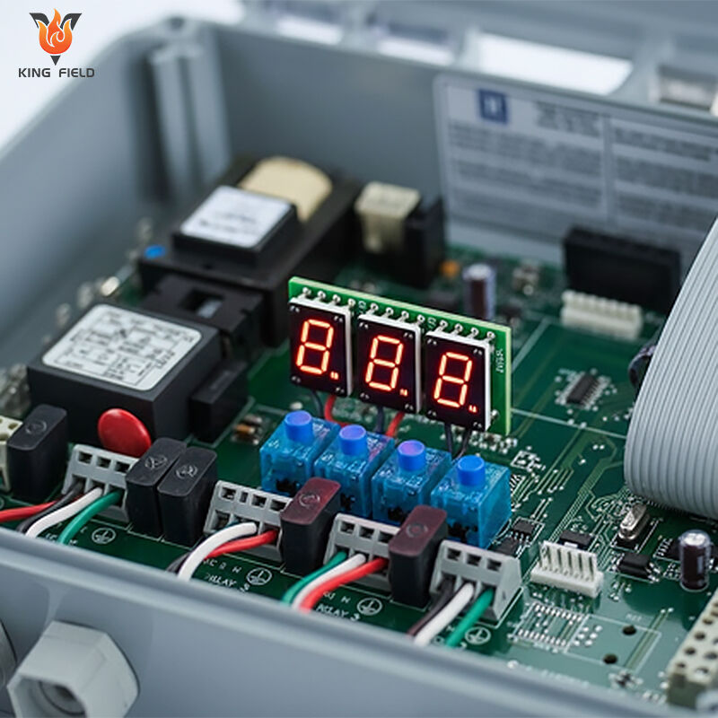
четирислойните PCB структури са идеални за компактна или преносима електроника, включително IoT сензори, медицински уреди и автомобилни модули, където по-плътното подреждане е от съществено значение за формфактора на продукта.
6. По-голяма механична якост
Структурната твърдост, осигурена от многослойната ламинация, гарантира, че печатната платка може да издържи на механични натоварвания при монтажа, вибрации и огъване в сурови условия.
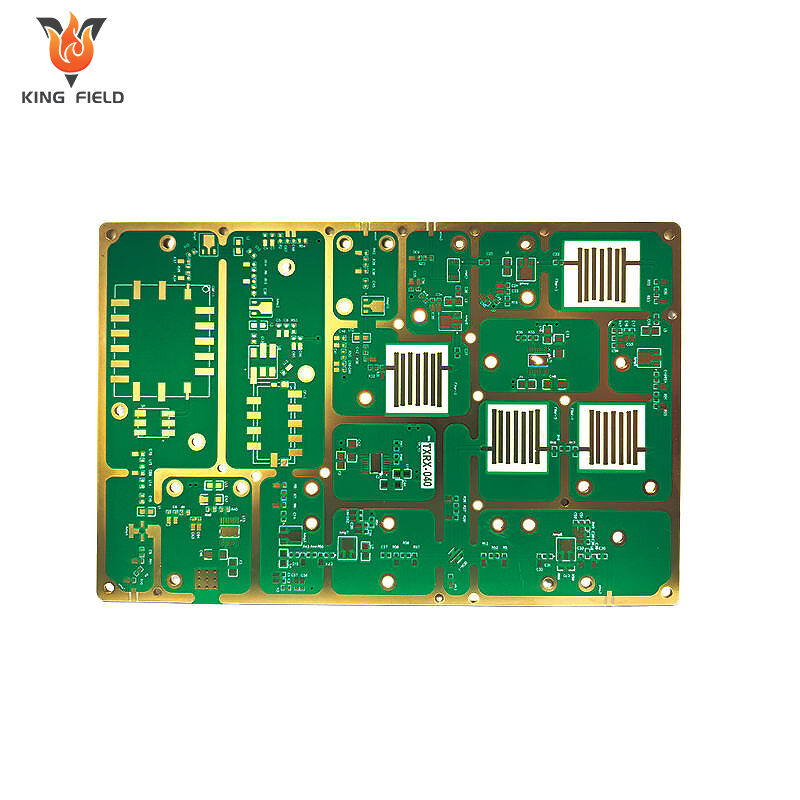
Типични сценарии за използване на 4-слойни PCB
- Модеми, домашна автоматизация и RF модули (по-добра EMC и сигнализация)
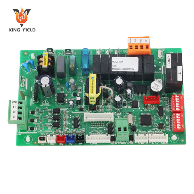
- Индустриални контролери и автомобилни ECU (издръжливост и надеждност)
- Медицински уреди (компактни размери, чувствителни към шум сигнали)
- Паметни часовници и носими устройства (висока плътност, малки размери)
Основни стъпки в процеса на производство на 4-слойни PCB
Разбиране на производствен процес на 4-слойна PCB стъпка по стъпка е от решаващо значение за всеки, ангажиран с проектиране, набавяне или осигуряване на качеството на PCB. В основата си производството на четири-слойни PCB е прецизен, многостепен процес, при който сурови медни ламинати, препрег и електронни проектни файлове се превръщат в здрав, компактен и готов за монтиране многослойен PCB.
Общ преглед: Как се произвеждат ключовите стъпки в 4-слойните PCB?
По-долу е показана обобщената последователност от процеси за производство на 4-слойни PCB, която може да служи като ръководство както за новодошлите, така и за опитните в индустрията:
- Проектиране на PCB и планиране на слоевете
- Подготовка на материали (избор на препрег, ядро, медна фолиа)
- Изобразяване и травиране на вътрешните слоеве
- Подравняване на слоевете и ламиниране
- Свредлене (CNC) и отстраняване на заострените ръбове по отворите
- Металопокритие на преходни отвори и галванизация
- Оформяне на външния слой (фотоотпорен слой, травиране)
- Нанасяне и затвърдяване на паялна маска
- Нанасяне на повърхностна обработка (ENIG, OSP, HASL и др.)
- Шелкова печат
- Форматиране на PCB (маршируване, рязане)
- Сглобяване, почистване и тестване (AOI/ICT)
- Финален контрол на качеството, опаковане и пратка
Следващото стъпка по стъпка ръководство задълбочено разглежда всяка област, като изяснява най-добрите практики, терминологията и уникалните характеристики на процеса за производство на четирислойни PCB .
Стъпка 1: Проектни съображения
Пътят на четирислойна PCB започва с екипа по инженерство, който дефинира изискванията на веригата, които след това се преобразуват в подробни проектни файлове – включително дефиниране на слоевете, подредба на слоевете и производствени изходни данни.
Основни елементи на дизайна на четирислойна PCB:
- Избор на структура на слоевете: Чести варианти като Сигнал | Заземяване | Енергия | Сигнал или Сигнал | Енергия | Заземяване | Сигнал. Изборът тук директно влияе върху електрическата производителност и възможността за производство.
-
Избор на материал:
- Ядро: Обикновено FR-4, макар че при проекти с висока честота и висока надеждност може да се използват Rogers, метални ядра или керамични субстрати.
- Препрег: Този армиран със стъклено влакно смолен материал е от решаващо значение за диелектричната изолация и механичната якост.
- Тегло на медта: 1 унция е стандарт; 2 унции и повече за захранващи площи или специални термични приложения.
- Планиране на контролиран импеданс: За проекти, предаващи сигнали с висока скорост или диференциални сигнали (USB, HDMI, Ethernet), изискванията за контролиран импеданс трябва да бъдат посочени според насоките на IPC-2141A.
-
Технология на преходни отвори:
- Чрезходови вии са стандартни за повечето четирислойни PCB платки.
- Слепи/закрити преходни отвори, обратно свредлене и запълване със смола са персонализирани опции за високоплътни или високочестотни платки; може да изискват последователно ламиниране.
-
Инструменти за проектиране на PCB Повечето проекти за 4-слойни PCB започват в професионални CAD инструменти:
- Altium Designer
- KiCad
- Autodesk Eagle Тези платформи генерират Gerber файлове и файлове за пробиване — стандартните цифрови чертежи, изпращани до производителя.
- Проверка на проектирането за производство (DFM): Извършват се DFM проверки, за да се гарантира, че всички елементи могат да бъдат произведени — проверява се проследяване/разстояние, съотношение на диаметър към дебелина на отвора, ширина на пръстена около отвора, маска за лепене, надписи и други. Ранна обратна връзка от DFM предотвратява скъпи преустройства или закъснения в производството.
Примерна таблица: Типични опции за структура на 4-слойна PCB
|
Опция за структура
|
Слой 1
|
Слой 2
|
Слой 3
|
Слой 4
|
Най-добър за
|
|
Стандартна (най-често срещана)
|
Сигнал
|
Заземен
|
Мощност
|
Сигнал
|
Контролиран импеданс, чувствителна към ЕМИ
|
|
Алтернативен
|
Сигнал
|
Мощност
|
Заземен
|
Сигнал
|
Управление на пътя на връщане
|
|
Високофренови
|
Сигнал
|
Заземен
|
Заземен
|
Сигнал
|
GHz+ вериги, превъзходна изолация
|
|
Персонализиран
|
Сигнал
|
Сигнал/Енергия
|
Заземен
|
Сигнал
|
Смесени вериги, напреднала настройка за ЕМС
|
Следваща стъпка
Следващата фаза в производствения процес на 4-слойни PCB iS Подготовка на материали —включително подбор на ядро, управление на пре-прег материали и почистване на ламинат.
Стъпка 2: Подготовка на материала
Избор на ядро и работа с медно покрит ламинат
Всеки висококачествен 4-слойен PCB започва с внимателен подбор и подготовка на основните си материали. Типична четири-слойна PCB използва ламинати с медно покритие —изолационни плоскости, ламинирани от двете страни с медна фолиа—като вътрешния „скелет“ на PCB.
Типове материали включват:
- FR-4 : Най-често срещаният тип, предлагат балансирано съотношение между цена и производителност за повечето приложения.
- FR-4 с висока температура на стъклен премин : Използва се за платки, изискващи по-голяма устойчивост на температура.
- Rogers, Teflon и ламинати за високи честоти : Указват се за ВЧ и микровълнови ПП при критични изисквания за ниски загуби и стабилни диелектрични свойства.
- Метална основа (алуминий, мед) : За силова електроника или приложения с високи топлинни изисквания.
- Керамика и CEM : Използват се в специализирани приложения с висока производителност.
Факт: Повечето многослойни печатни платки в потребителската, медицинската и промишлената електроника използват стандартни FR-4 ядрени слоеве с тегло на медта 1 унция като отправна точка, оптимизирани по отношение на цена, производимост и електрическа надеждност.
Рязане на ламинатите до размер на панела
Производствените линии за ПП обработват платките в големи панели, които след това се разделят на отделни печатни платки след нанасяне на веригата и монтаж. Прецизното рязане на медта покритите ламинати и листовете препрег осигурява еднородност, максимизира добива от материала и съответства на практиките за панелиране за най-добра икономическа ефективност.
Употреба на препрег при стекиране на слоеве
Препрег (предварително импрегнирани композитни влакна) е по същество лист от стъклотекстурирана материя, импрегнирана с частично затопряна епоксидна смола. По време на ламинация препрегът се поставя между медни слоеве и ядра, като изпълнява функция както на диелектрик (осигурява необходимата изолация), така и на адхезив (разтапя се и залепва слоевете при нагряване).
Ключови технически точки:
- Съвместимост на дебелината на диелектрика: Плъстовете и дебелината на основата се адаптират, за да се постигнат целевите дебелини на платката — например 1,6 мм за стандартни 4-слойни PCB структури.
- Диелектрична константа (Dk): Съвременните приложения (особено RF/високоскоростни цифрови) изискват добре характеризирани прегрети материали; стойностите на Dk директно влияят върху импеданса на проводниците.
- Спротивляване на влажност: Висококачественият плъст минимизира абсорбцията на вода, която в противен случай може да повлияе на електрическите свойства и надеждността.
Предварително почистване на медната повърхност
Важна, но често пренебрегвана стъпка при изработването на четирислойни PCB е предварителното почистване на медните повърхности върху основата и фолиоматериалите:
- Чистене с четка и микротравене: Материалите се подлагат на механично почистване с четка, след което се потапят в слаба киселина или химически микротравител. Това премахва оксидите, смолите и микрочастиците от повърхността, като разкрива чиста мед за последващото образуване на образа.
- Изсичане: Всяка остатъчна влага може да отслаби адхезията или да причини отделяне на слоевете, затова платките се суши внимателно.
Проследимост и контрол на материали
На този етап професионалният Производители на ПЛС присвоява партидни номера на всяка платка и всяка партида материал. Следяемост е от съществено значение за спазване на стандарти за качество (ISO9001, UL, ISO13485) и за проследяване на проблеми в редките случаи, когато възникнат след доставка.
Таблица: Типични материали и спецификации за стандартна 4-слойна PCB
|
Материал
|
Употреба
|
Типични спецификации
|
|
FR-4 основа
|
Субстрат
|
0,5 – 1,2 mm, 1 oz Cu
|
|
Предварително напитан
|
Диелектрични
|
0,1 – 0,2 mm, Dk = 4,2 – 4,5
|
|
Медна Фолия
|
Проводимо
|
1 oz (35 µm) стандарт; 2 oz за захранващи слоеве
|
|
Паян лак
|
Защита
|
Зелен, 15–30 µm дебелина, тип LPI
|
|
Шелковоплетенски чернила
|
Маркировки
|
Бяло, повдигнато <0.02 mm
|
Правилната подготовката на материала е основата за надежден 4-слойен PCB. След това преминаваме към следващ етап с голямо техническо значение: Изображение и травиране на вътрешния слой.
Стъпка 3: Изображение и травиране на вътрешния слой
Вътрешните вериги на 4-слойен PCB — обикновено заземяване и захранване, или допълнителни сигнали при специализирани структури — формират електрическия скелет за цялото проследяване на сигнали и разпределение на енергия. Точно в тази стъпка цифровият дизайн на платката се реализира физически с точност под милиметър върху истинско медно покритие.
1. Почистване: Подготовка на повърхността
Преди заснемането предварително почистените медни ядра (подготвени в предишната стъпка) преминават през окончателно изплакване и микротравиране. Този химичен процес премахва последните следи от окисление, увеличава микроскопската шероховатост на повърхността и осигурява оптимална адхезия за фотосъпротивата. Всякакви остатъчни замърсители — дори и най-малките — могат да доведат до недостатъчно травиране, прекъсвания/къси съединения или лошо качество на отпечатъка.
2. Нанасяне на фотосъпротива
Очистените медни ядра след това се покриват с фотоотпор —фоточувствителна полимерна пленка, която осигурява точно дефиниране на веригата. Нанасянето обикновено се извършва чрез ламинарен процес със суха филмова пленка , при който фотолакът плътно се залепва за медта под загряващи валцове.
-
Видове:
- Отрицателен фотолак е индустриалният стандарт за многослойни платки; експонираният слой се крос-линква и остава след проявяването.
- Течен фотолак може да се използва в някои процеси за по-точен контрол, макар че сухата пленка е преобладаваща при производството на повечето четирислойни PCB платки.
3. Експониране (UV визуализация / Фотоформи)
След това подготовката минава през автоматизирана UV машина за визуализация , където високорезолюционен лазер или фотомаска, генерирана чрез CAD, подравнява схемите на веригите върху медното плато. Ултравиолетова светлина преминава през прозрачните части на маската:
- Където маската е прозрачна : Фоточувствителният слой се експонира и полимеризира (затвърдява).
- Където маската е непрозрачна : Фоточувствителният слой остава мек и неекспониран.
4. Развиване (Извличане на неекспонирания слой)
Платото се развива — потапя се в лек воден разтвор (развивател). Неекспонираният, мек фоточувствителен слой се измива, като по този начин се оголва медта отдолу. Остава само схемата на веригата (сега твърд, експониран слой), точно съответстваща на проекта, предоставен в Gerber файловете.
5. Травлене (Премахване на мед)
След това печатната платка минава през травене на вътрешния слой —контролиран процес на киселинно травене, обикновено с използване на амонячен или разтвор на желязен хлорид:
- Травенето премахва нежеланата мед от области, които не са защитени от затвърденото фотопроявително вещество.
- Остават веригите, контактните площи, равнините и други проектирани медни елементи.
6. Премахване на резиста
След като желаните медни модели са разкрити, затвърденият фотопроявител, който ги предпазва, се премахва с отделен химичен разтвор. Остават голи, лъскави медни вериги, точно съответстващи на проекта на вътрешния слой.
Контрол на качеството: автоматизирана оптична инспекция (АОИ)
Всеки вътрешен слой се проверява стриктно за дефекти чрез Автоматичен оптичен инспекционен (AOI) . Високоразрешаващи камери сканират за:
- Отворени вериги (прекъснати проводници)
- Недоетчирани или прекомерно етчирани елементи
- Къси съединения между проводници или контактни площи
- Грешки в подравняването или регистрирането
Защо етчирането на вътрешния слой е критично за 4-слойни PCB
- Сигнална цялостност: Чисти и добре етчирани вътрешни площи осигуряват стабилна референция за високочестотни мрежи, предотвратявайки шум и ЕМИ.
- Разпределение на енергия: Широките захранващи площи минимизират пада на напрежение и разсейването на мощността.
- Непрекъснатост на плочата: Поддържането на широки, непрекъснати площи отговаря на IPC-2221/2222 и намалява отклонението на импеданса.
"Точността на този етап определя работоспособността на платката. Единичен къс или отворен контакт във вътрешен захранващ или заземяващ слой води до пълен отказ след ламинация — невъзможно за ремонт. Затова водещите производители на PCB поставят под контрол процесите на образуване и автоматичен оптичен инспекционен контрол (AOI)." — kINGFIELD
Стъпка 4: Подравняване на слоевете и ламиниране
Правилно подравняване и ламиниране са от съществено значение при производството на 4-слойни PCB. Този процес физически свързва предварително заснетите медни слоеве (които вече съдържат вътрешните вериги и площи) с листове препрег и външни медни фолиа — създавайки крайния четири-слоен пакет.
A. Подготовка на пакета: Подредба на слоевете
Производствената линия сега сглобява вътрешната структура, използвайки:
- Вътрешни ядра: Готови (изтравани, почистени) вътрешни ядра — обикновено слоеве за заземяване и захранване.
- Препрег: Точно измерени диелектрични (изолационни) слоеве, поставени между медните ядра и външните медни фолиа.
- Външни медни фолиа: Листове, които ще станат горен и долен маршрутизиращи слоеве след заснемането на веригата.
Б. Закачване и регистрация (съвпадане на слоеве)
Съвпадането не е само механично изискване – то е от съществено значение за:
- Поддържане на точното съвпадане между контактните площи и преходните отвори, така че пробитите по-късно дупки да не пропускат, да не прерязват или да не предизвикват късо съединение със съседни елементи.
- Задържане на референтните равнини точно под критичните сигнали, за да се осигури цялостността на сигнала и контролирания импеданс.
Как се постига съвпадането:
- Закачване: Чрез пакета от слоеве се пробиват прецизни стоманени щифтове и отвори за регистрация, за да се фиксират всички плочи в абсолютно съвпадение по време на сглобяването.
- Оптична регистрация: Напредналите производители на PCB използват автоматизирани оптични системи за проверка и подобряване на съвпадането между слоевете, като често постигат допуск от ±25 μm (микрона).
В. Ламиниране: Сливане чрез топлина и налягане
След това нареденият и фиксиран пакет се зарежда в гОРЕЩА ПРЕСА ламинарен апарат:
- Вакуумен етап: Премахва уловения въздух и летливи остатъци, предотвратявайки разслояване или образуване на мехурчета.
- Топлина и налягане: Препрегът омеква и се разтваря при температури от 170–200 °C (338–392 °F) и налягане от 1,5–2 MPa.
- Вулканизация: Омекналата смола в препрега запълва микропразнините и свързва слоевете заедно, след което се затвърдява (полимеризира) при охлаждане.
Резултатът е единичен твърд, залепен панел —с четири отделни, електрически изолирани медни слоя, перфектно ламинирани и готови за допълнителна обработка.
Контрол на качеството: Инспекция и тестване след ламиниране
След ламинирането, панелът се охлажда и почиства. Основните проверки за контрол на качеството включват:
- Измерване на дебелина и огъване: Осигурява равнинност на платката и съответствие с предварително зададените допуски (обикновено ±0,1 мм).
-
Деструктивен анализ на напречни сечения: Пробни платки се нарязват и анализират под микроскоп, за да се провери:
- Изолация между слоевете (без разслояване, празноти или недостиг на смола).
- Регистрация на слоевете (точност между отделните слоеве).
- Качество на залепването на границите между препрег и ядро.
- Визуална проверка: Проверка за разслояване, деформация и замърсяване на повърхността.
Стандарти и най-добри практики на IPC
- IPC-6012: Определя изисквания за производителност и инспекция за твърди ППП, включително подравняване на повече слоеве и качество на ламиниране.
- IPC-2221/2222: Препоръчва непрекъснати площи, минимални отвори и строги допуски за позициониране за надеждна работа.
- Материали: Използвайте суровини за ППП от промишлен клас — препрег, ядро и мед, предпочтително с проследими партидни номера за контрол на качеството и регулаторно отчитане.
Обобщаваща таблица: Предимства на прецизното ламиниране при четирислоен ППП
|
Полза
|
Подробности
|
|
Висша сигнална цялост
|
Осигурява правилните взаимоотношения между заземяване/сигнални площи
|
|
Надеждни междусвръзки
|
Гарантира, че пробитите преходи ще достигнат всички необходими контактни площи/слоеве
|
|
Механична издръжливост
|
Издръжливо на термични/механични напрежения при сглобяване/използване
|
|
Намалено EMI
|
Минимизира отместването на слоевете, предотвратяващо „горещи точки“ от ЕМИ
|
|
Производствена годност
|
По-малко дефекти, по-ниски отпадъци, по-добра икономическа ефективност
|
Стъпка 5: Свредлене и металопокритие
The етап на свредлене и металопокритие при производството на четирислойна PCB етап, на който истински оживяват физическата и електрическата свързаност на платката. Точното формиране на преходни отвори и здраво електролитно покритие с мед са от съществено значение за надеждна предаване на сигнали и мощност в многослойни структури.
A. CNC Свредлене на преходни отвори и отвори за компоненти
Съвременното производство на четирислойни PCB използва машини за компютърно управление (CNC) за създаване на стотици или дори хиляди отвори на панел – осигурявайки точност, скорост и повтаряемост, които са от решаващо значение за напредналите приложения.
Типове отвори в четирислойни PCB:
- Чрез-слоеви виаси: Простират се напълно от горния слой до долната страна, свързвайки всеки меден слой и равнина. Те са основата за сигнали и заземяване.
- Отвори за компоненти: Падове за компоненти с чрез-слоева монтаж (THT), съединители и щифтове.
-
По избор:
- Слепи виаси: Свързват външен слой с един (но не и двата) вътрешни слоя; по-малко разпространени при 4-слоеви платки поради по-високата цена.
- Погребани виаси: Свързват само вътрешни слоеве; използват се при проекти с висока плътност или комбинирани твърдо-еластични PCB.
Характеристики на процеса на пробиване:
- Нагласяне на панела: Множество панели могат да бъдат пробити едновременно, за да се оптимизира производителността, като всяка от тях е поддържана от фенолна входно-изходна плоча, която предотвратява образуването на ръбове или отклонение при пробиването.
- Избор на свредла: Свредла от карбид или с диамантено покритие с размери от 0,2 мм (8 mils) нагоре. Износването на свредлата се следи стриктно и те се заменят през точно определени интервали за постигане на висока последователност.
- Допуснато отклонение в положението на отвора: Обикновено ±50 µm, което е задължително за точното подравняване на преходните контактни площи при високоплътни конструкции.
Б. Отстраняване на ръбовете и премахване на замазванията
След завършване на пробиването механичната обработка оставя неравни ръбове (ръбове) и епоксидни „замазвания“ по стените на преходния отвор, особено там, където са изложени стъклени влакна и смола. Ако не се обработят, те могат да блокират металопокритието или да причинят проблеми с надеждността.
- Премахване на застилки: Механичните четки премахват остри ръбове и парчета фолио.
- Премахване на замазванията: Панелите се обработват химически (с използване на калиев перманганат, плазма или методи без перманганат), за да се отстранят остатъците от смола и напълно да се изложат стъклените влакна и медта за последващо метално свързване.
C. Формиране на преходни отвори и медно галванизиране
Може би най-критичната стъпка — гравиране на преходни отвори —създава изключително важните електрически канали между слоевете на 4-слоен PCB.
Процесът включва:
- Почистване на стените на отворите: Панелите преминават през предварителна обработка (киселинно почистване, микротравене), за да се осигурят напълно чисти повърхности.
- Химично нанасяне на мед: Тънък слой (~0,3–0,5 µm) мед се нанася химически върху стените на отворите, „засявайки“ преходния отвор за последващо галванизиране.
- Электроплакат: PCB панелите се поставят в медни бани. Прилага се постоянен ток (DC); медните йони се отлагат върху всички оголени метални повърхности – включително стените на преходните отвори и проходните отвори – като създават равномерна, проводима медна тръба във всеки отвор.
- Стандартна дебелина на медта: Готовите чрезстенни отвори обикновено се покриват с минимум 20–25 µm (0.8–1 mil), съгласно IPC-6012 Class 2/3 или спецификации на клиента.
- Проверки за еднородност: Използват се сложни методи за контрол на дебелината и напречни сечения, за да се гарантира липсата на тънки участъци или празноти, които биха могли да причинят прекъснати вериги или прекъсвани повреди в експлоатация.
Контрол на качеството:
- Анализ на напречни сечения: Изследват се извадени отвори, които се разрязват и измерват по дебелина на стената, адхезия и еднородност.
- Тестове за непрекъснатост: Електрическите проверки гарантират, че всеки чрезстенен отвор осигурява здрава връзка от контакт към контакт, слой към слой.
D. Защо пробиването и металопокритието са важни за 4-слойни PCB
- Висока надеждност: Еднородно, бездефектно металопокритие на чрезстенните отвори предотвратява прекъснати/къси съединения и фатални повреди в експлоатация. - Целост на сигнала: Правилното оформяне на преходни отвори поддържа бързи преходи на сигнала, връщане по път с ниско съпротивление и надеждно захранване. - Разширена поддръжка при проектирането: Осигурява по-фини размери на елементите, плътно опаковане и съвместимост с технологии като HDI или комбинирани твърдо-еластични PCB платки.
Таблица: Параметри за пробиване и металопокритие за стандартни 4-слойни PCB платки
|
Параметър
|
Типична стойност
|
Забележка
|
|
Мин. крайни размери на отвора
|
0,25–0,30 mm (10–12 mil)
|
По-малки за HDI/напреднали процеси
|
|
Дебелина на медта в стената на отвора
|
≥ 20 µm (0,8 mil, IPC-6012)
|
До 25–30 µm при спецификации за висока надеждност
|
|
Чрез съотношение на аспекта
|
До 8:1 (дебелина на платка : отвор)
|
По-високи съотношения изискват внимателен DFM
|
|
Еднородност на металопокритието
|
±10% по цялата плоча
|
Контролира се чрез тестови купони/рентген
|
Стъпка 6: Формиране на външния слой (създаване на верига на слоеве 1 и 4)
The външни слоеве на вашата 4-слойна PCB — слоеве 1 (горен) и 4 (долен) — съдържат контактните площи, проводници и медни елементи, които ще взаимодействат директно с компонентите или свързващите елементи по време на монтаж. Този етап е подобен по смисъл на обработката на вътрешните слоеве, но изискванията са по-високи: тези слоеве подлежат на значително леене на припой, почистване и износване и трябва да отговарят на най-строгите косметични и размерни стандарти.
A. Нанасяне на фоточувствителен слой за външните слоеве
Както при вътрешните слоеве, външните медни фолиа първо се почистват и микротравят, за да се получи чиста повърхност. След това върху всяка повърхност се нанася слой фотоотпор (обикновено сух филм) чрез ламиниране с нагрети валчета, за да се осигури залепване.
- Факт: Производителите на висококачествени PCB внимателно контролират дебелината на филма и налягането при ламинацията, за да гарантират последователно формиране на изображението и минимизиране на деформациите по ръбовете.
Б. Иматаж (Фотошаблон/Директно лазерно UV иматаж)
- Фотошаблон: При повечето серийни производстви фотомаски, съдържащи шаблоните на медните проводници и площадки за горния и долния слой, се насочват оптически спрямо пробитите отвори.
- Лазерно директно изобразяване (LDI): При високоточни или бързи поръчки компютърно управляван лазер „записва“ директно върху платката следите и площадките, дефинирани в Gerber, с точност на микрони.
- Ултравиолетовата (UV) светлина полимеризира експонирания фотополимер, фиксирайки точно външната електрическа верига на мястото ѝ.
В. Разработване и травене
- Развитие: Неекспонираният фотополимер се измива с лек алкален разтворител, като се оголва медта, която ще бъде изтравена.
- Киселинно травене: Оголеният мед се отстранява чрез етчерни конвейери с висока скорост, като се запазват само следите, контактните площи и оголените вериги, защитени от затвърдения фоторезист.
- Почистване чрез обработване с разтвор Оставащият фоторезист се премахва, разкривайки свежи, лъскави външни медни структури, които формират повърхности за запояване и токопроводящи следи за вашата платка.
Таблица: Основни размери за структуриране на външните слоеве на 4-слойна PCB
|
Функция
|
Стандартна стойност
|
Забележка
|
|
Широчина на проводници
|
0,15–0,25 mm (6–10 mil)
|
За повечето цифрови, захранващи и смесени сигнали проекти
|
|
Пространство
|
0,15–0,20 mm (6–8 mil)
|
Контролирани за IPC Class 2/3
|
|
Кръгова пръстена
|
≥0,1 mm (4 mil)
|
Зависи от DFM, осигурява надеждни запоени възли
|
|
Допуск между падове
|
±0,05 мм (2 mil)
|
За високоплътни LSI/SMT
|
D. Инспекция и проверки за качество
Ново гравираните панели се инспектират визуално и чрез AOI (Автоматизирана оптична инспекция) за:
- Прекомерно или недостатъчно гравирани проводници и площи
- Мостове или къси съединения
- Отворени или липсващи елементи
- Регистрация/подравняване с предварително пробити преходни отвори
Защо структурирането на външния слой е важно за 4-слойни PCB
- Надеждност при монтаж: Паялността, размерът на контактните площи и устойчивостта на проводниците се определят именно тук.
- Сигнална цялостност: Високочестотни сигнали, диференциални двойки и мрежи с контролирано вълново съпротивление завършват на тези слоеве, което прави прецизното дефиниране на следите от решаващо значение.
- Токоизносяне: Остава достатъчно мед за всички нужди от маршрутизация и отвеждане на топлината.
Стъпка 7: Паялна маска, повърхностна обработка и шелакова печат
След като приключите с моделирането на медта за външните слоеве на вашия 4-слойна PCB, е време да осигурите издръжливост, паялност и яснота както за монтажа, така и за поддръжката по-късно. Тази многоетапна стъпка отличава професионалното производство на многослойни платки, като защитава веригата, гарантира надеждно запояване и осигурява лесна визуална идентификация.
A. Нанасяне на паялна маска
The паян лак е защитно полимерно покритие — типично зелено, макар че също толкова популярни са синьо, червено, черно и бяло — нанасяно върху горната и долната повърхност на PCB:
-
Цел:
- Предотвратява образуването на паялни мостове между близко разположени площи и проводници.
- Предпазва външните електрически вериги от окисляване, химическо въздействие и механично изтриване.
- Подобрява електрическата изолация между проводниците, което допълнително подобрява цялостността на сигнала и намалява ЕМИ.
Процес на прилагане:
- Покритие: Панелът е покрит с течен фоточувствителен (LPI) лак за запояване, който покрива всичко освен медните площадки, които по-късно ще бъдат запоявани.
- Изображение и експониране: Ултравиолетова светлина се използва с маска за изработване на шаблон, за да се дефинират отвори (за площадки, тестови точки, преходни отвори).
- Разработка: Неекспонираният лак за запояване се измива, докато експонираният се затвърдява и предпазва електрическите вериги.
- Отвръзване: Панелите се изпечват или облъчват с UV, за да се напълно затвърди лакът.
Б. Опции за повърхностна обработка
За да се гарантира, че всички оголени площадки издържат на съхранение, устояват на окисляване и осигуряват безупречно запояване по време на монтаж, се нанася повърхностно завършване се прилага. Има няколко вида обработки, подходящи за различни приложения, разходи и изисквания за монтаж:
|
Повърхностно завършване
|
Акроним
|
Ключови предимства
|
Типични случаи на употреба
|
|
Безелектролитен никел с имерсионно злато
|
ENIG
|
Плосък, устойчив на окисляване, подходящ за фини стъпки/BGA; отлична лепливост, съвместим с RoHS
|
Висока надеждност, HDI, потребителски, RF
|
|
Органично покритие за запазване на лепливостта
|
OSP
|
Чист, без олово, икономичен; предпазва пресен мед и е лесен за лепене чрез рефлукс
|
Масов пазар, прост SMT
|
|
Имерсионно калай
|
—
|
Плосък, добър за притискане или високоскоростни конектори
|
Контролируем импеданс, платки с притискане
|
|
Потапяне в сребро
|
—
|
Отличен за висока честота/цялостност на сигнала
|
RF, високоскоростен дигитален
|
|
Нивелиране с топъл въздух / Безолово HASL
|
HASL
|
Широко използван, икономичен, здрав; разтопено оловно покритие
|
Обща електроника, комбинирана THT/SMT
|
- ENIG е стандарт в индустрията за повечето 4-слойни прототипни и серийни платки, особено когато има значение равнинността на повърхността и високата плътност (BGA, LGA, QFN).
- OSP е най-подходящ за безоловна битова електроника, която изисква икономическа ефективност и добро качество на спойките.
Разлики между ENIG и HASL:
- ENIG осигурява по-гладка и по-равна повърхност, необходима за ултрафини стъпки и BGA.
- HASL създава неравни „куполи“, които може да не отговарят на съвременната високоплътна сглобка на PCB.
- ENIG е по-скъп, но осигурява по-добро дългосрочно съхранение и съвместимост с ожичаване.
C. Шелкографско печатане
С приложен лак за лепене и завършена повърхност, последният слой е силк스크рийн —използва се за маркиране на:
- Контури и етикети на компоненти (R1, C4, U2)
- Маркери за полярност
- Референтни обозначения
- Индикатори за пин 1, лога, кодове за ревизия и баркодове
Контрол на качеството: окончателна AOI и визуални проверки
- Автоматична оптична инспекция (AOI): Осигурява правилния размер/позиция на отворите в лака, липсата на случайни следи от лак и коректното излагане на контактните площи.
- Визуална проверка: Потвърждава яснотата на шелкографията, липсата на липсващо мастило, липсата на лак върху основни елементи и проверява цялостността на повърхностната обработка.
Защо този етап е важен за 4-слойни PCB
- Паяене: Само изложените контактни площи / точки са достъпни за паяене; маскирането на останалата част предотвратява случайни мостове — критично при плътни конструкции.
- Устойчивост към корозия и замърсяване: Срокът на служба и надеждността на платката се подобряват значително чрез защита на медните повърхности от въздух, влага и пръсти.
- Намаляване на грешките: Ясни и точни маркировки намаляват грешките при монтаж, необходимостта от преработка или времето за сервизно обслужване на терен.
Стъпка 8: Профилиране, монтаж и почистване на PCB
След като всички слоеве на веригата са фиксирани, чрезплатинираните преходни отвори, нанесения слой за маскиране на лепене и повърхностната обработка, сега фокусът се премества към оформянето, попълването и почистването на 4-слойна PCB тази фаза превръща многослоевия вилица от прецизно изработен, но недиференциран блок в специфично по форма, напълно сглобено функционално устройство.
A. Профилиране на PCB (рязане и маршрутизиране)
На този етап множество образи на PCB се намират на по-голяма производствена вилица. Профилиране означава отделянето на всяка четирислойна печатна платка до необходимия контур, включително изрязвания, процепи или V-жлебове.
Основни методи:
- Фрезиране чрез CNC : Високоскоростни карбидни фрези точно следват външния ръб на платката, отговаряйки на толерантни спецификации до ±0,1 мм.
- V-набиване : Повърхностни жлебове позволяват лесно отделяне на платките чрез счупване по линиите на набиване.
- Ударяне : Използва се за серийно производство на платки със стандартна форма, за оптимизиране на пропускателната способност.
Б. Монтаж на печатни платки (SMT и THT поставяне на компоненти)
Повечето четирислойни PCB платки днес използват монтаж с комбинирани технологии, като използват както Технология за повърхностно монтиране (SMT) за висока плътност и автоматизирано залепване, така и Технология с преходни отвори (THT) за високопроизводителни конектори, захранващи елементи или остарели компоненти.
1. SMT монтаж
- Тампонно печатане : Пастообразен припой се нанася чрез екранна печат на площи с помощта на лазерно изрязани шаблони за прецизен обем.
- Поставяне с пипало : Автоматизирани машини поставят до десетки хиляди компонента на час с точност от ниво микрони — дори за пасивни 0201, QFN, BGA или LSI устройства.
- Рефловна паян : Попълнените PCB минават през принудително вентилирана фурна с точно зададен температурен профил, където последователно се стопява и охлажда припоят. Това създава здрави спойки за всички SMT устройства.
2. THT монтаж
- Ръчно или автоматизирано вмъкване : Компоненти с дълги изводи, като конектори или големи електролитни кондензатори, се вкарват през металнизираните отвори.
- Вълново паяне : Платките преминават над вълна от разтопен припой, за да бъдат спояни едновременно всички вкаране изводи — проверен метод за постигане на висока механична устойчивост.
SMT срещу THT:
- SMT осигурява висока плътност, лека тегло и компактни сборки. Най-подходящ за съвременни многослойни PCB.
- THT все още се предпочита за конектори и високомощни части, които изискват допълнително закрепване.
C. Почистване (изопропилов алкохол и специализирани почистващи средства за PCB)
След запояване остатъците като флюс, топчета от припой и прах могат да намалят надеждността, особено върху плътно разположените проводници и преходни отвори на четирислойни печатни платки.
Етапи на процеса:
- Почистване с изопропилов алкохол (IPA) : Често използван при прототипиране и малки серии, ръчно премахва йонни остатъци и видим флюс.
- Автоматични почистващи машини за PCB : Промишлени машини използват деионизирана вода, сапунисващи агенти или специализирани разтворители за почистване на множество платки едновременно – важно за медицинската, военната и автомобилната индустрия.
Защо почистването е важно:
- Предотвратява корозия и образуване на дендрити между елементите на веригата.
- Намалява риска от течове в електрическата изолация, особено при високоомни или високонапрежни вериги.
Таблица: Обобщение на процеса на монтаж и почистване
|
Сцена
|
Техника
|
Предимства
|
Типични приложения
|
|
Профилиране
|
CNC маршрутизация, V-резки
|
Прецизност, ръбове без напрежение
|
Всички типове платки
|
|
SMT монтаж
|
Щамп/Рефлоу
|
Висока плътност, скорост, точност
|
Масов пазар, висока плътност
|
|
THT сборка
|
Вълново паяне
|
Издръжливи съединения, подходящи за обемисти части
|
Електрозахранване, свързващи елементи
|
|
Почистване
|
IPA или линеен уред за измиване
|
Премахва остатъците, осигурява надеждност
|
Всички, особено критични
|
Стъпка 9: Финално тестване, контрол на качеството (QC) и опаковане
A 4-слойна PCB е толкова добро, колкото е стриктността на тестовете и контрола на качеството. Дори ако изглежда перфектно на око, невидими дефекти — прекъснати вериги, къси съединения, несъответствия или недостатъчно галванично покритие — могат да причинят неравномерно поведение, ранни повреди или рискове за безопасността. Затова водещите производители на PCB използват всеобхватен набор от електрически, визуални и документирани проверки, подкрепени от международно признатите стандарти IPC.
A. Автоматизирана оптична инспекция (AOI)
Автоматичен оптичен инспекционен (AOI) се извършва многократно по време на производството на многослойни PCB, като най-критичната фаза е след финалната сглобка и леене.
- Как работи: Камери с висока разделителна способност сканират двете страни на всяка PCB, сравнявайки всеки проводник, контактна площадка и леен възел с цифровите Gerber файлове.
-
Какво открива AOI:
- Прекъснати вериги (прекъснати проводници)
- Къси съединения (свързващи мостове от лой)
- Липсващи или изместени компоненти
- Заварени възли с недостатъчен или излишен припой
- Появата на 'гробници' или несъосване на компонентите
Б. Проверка по верига (ICT)
Тест вътре в веригата (ICT) е златният стандарт за проверка на функционалността на монтирани 4-слойни PCB:
- Контактни проби: Тестери тип 'легло от нокти' или летящи проби осъществяват контакт със специални тестови точки или изводи на компоненти.
- Тестови скриптове: Подават сигнали през веригата и измерват отговорите в ключови възли.
-
Проверявани параметри:
- Непрекъснатост между всички сигнали и точки за захранване
- Съпротивление/емност на ключови мрежи
- Цялостност на преходни отвори и металоизолирани отвори
- Наличие/отсъствие и ориентация на основните компоненти
ICT позволява:
- Незабавна диагностика на ниво платка (локализиране на дефектни спойки, прекъсвания или неправилно поставени компоненти)
- Статистически данни за групи продукти за наблюдение на процеса
В. Електрически тестове
Всеки завършена четирислойна PCB подлежи на пълен електрически тест за непрекъснатост „къси съединения и прекъсвания“. На този етап:
- Електрически тест (ET): Високо напрежение се прилага към всички проводници и връзки.
- Цел: Откриване на скрити „обриви“ (прекъсвания) или „къси съединения“ (непреднамерени мостове), независимо от визуалния вид.
За конструкции с контролиран импеданс:
- Импедансни проби: Тестови проводници, изработени със същата структура и процес като серийните мрежи, позволяват измерване и валидиране на характеристичния импеданс (например 50 Ω единично, 90 Ω диференциално).
D. Документация и проследяемост
- Gerber, файлове за свредлене и тестови файлове: Производителят събира и архивира всички ключови данни, осигурявайки пълна проследяемост от партидата материали до готовата платка.
- Чертежи за монтаж и сертификати за качествен контрол: Прилагат се към доставките с висока надеждност за спазване на стандарти ISO9001/ISO13485, медицински или автомобилни стандарти.
- Баркодиране: Сериените номера и баркодовете се отпечатват върху всяка платка или панел за проследяване, диагностика и препратка към „цифров двойник“.
Е. Финална визуална проверка и опаковане
Обучени инспектори извършват последна проверка с помощта на увеличение и високоинтензивно осветление, за да огледат критични елементи:
- Чистота на контактните площадки и виите (без оловни топчета или остатъци)
- Маркировки, яснота на етикетирането, ориентация и точност на кода за ревизия
- Качество на ръба и профилирането (без разслоения, чипове или повреди)
Опаковка:
- Вакуумно запечатани антистатични торбички предпазват от ЕСР и навлизане на влага
- Балончета, пяна или персонализирани кутии предпазват от физически удар по време на пратка
- Всеки лот се опакова според инструкциите на клиента, включително силикагелови пакети или индикатори за влажност за пазари с висока надеждност
Таблица: Изпитвателни и контролни стандарти за 4-слойни PCBs
|
Тестове/Проверка
|
Стандарт/референция
|
Какво гарантира
|
|
AOI
|
IPC-610, ISO9001
|
Видимо без дефекти при изработката
|
|
Електрически тест (ET)
|
IPC-9252
|
Без къси съединения/обриви
|
|
ICT/Летяща проба
|
По поръчка/IPC-2222
|
Функционалност, тест по конкретни пинове
|
|
Проверка на импеданс
|
IPC-2141A, купони
|
Съответствие на линията за предаване
|
|
Визуален контрол
|
IPC-A-610, ISO13485
|
Качество на външен вид и механична изработка
|
Как да създадете 4-слоен структурен пакет в Altium Designer
Контролиране на вашите 4-слойна PCB структура е от съществено значение за постигане на правилния баланс между електрическите характеристики, производимостта и разходите. Съвременни инструменти за проектиране на PCB като Altium Designer предоставят интуитивни, мощни интерфейси за задаване и последващо експортиране на всички детайли, необходими на производителите за качествено и надеждно производство на многослойни PCB.
Стъпка по стъпка: Определяне на 4-слойната PCB структура
1. Започнете проекта си в Altium
- Отворете Altium Designer и създайте нов PCB проект.
- Внесете или начертайте вашите схеми, като сте сигурни, че всички компоненти, мрежи и ограничения са дефинирани.
2. Достъп до управлението на слоевете
- Отиди на Design → Layer Stack Manager.
- Управлението на слоевете ви позволява да конфигурирате всички проводими и диелектрични слоеве, дебелини и материали.
3. Добавяне на четири медни слоя
- По подразбиране ще виждате горен слой и долен слой.
- Добави два вътрешни слоя (обикновено с имена MidLayer1 и MidLayer2) за вашата четирислойна конструкция.
4. Определяне на функциите на слоевете
Задайте обичайни цели за всеки слой, както следва:
|
Слой
|
Типична функция
|
Пример със стекване
|
|
Връх
|
Сигнал + Компоненти
|
L1 (Сигнал)
|
|
МидЛаер1
|
Равнина на земята
|
L2 (Основа)
|
|
МидЛаер2
|
Плоскост за захранване (VCC и др.)
|
L3 (Захранване)
|
|
Дъно
|
Сигнал / Компоненти
|
L4 (Сигнал)
|
5. Настройка на дебелината на диелектрика/препрег и основата
- Щракнете между слоевете, за да зададете дебелината на диелектрика (препрег, основа) чрез стойности, определени от производителя .
- Типична обща дебелина за 4-слойна PCB: 1.6mm (но може да бъде по-тънка/по-дебела според нуждите).
- Въведете стойности за диелектрична константа (Dk) и тангенс на загубите, особено при проекти с контролиран импеданс.
6. Задаване на медно тегло
- Посочете дебелината на медта за всеки слой: обикновено 1 унция/кв. фут (~35 μm) е стандартна за сигнали; 2 OZ или повече при високи токове.
- Тези стойности влияят на изчисленията за широчината на проводниците и механичната издръжливост.
7. Активиране на изчисления за импеданс
- Използвайте вграденото Калкулатор за импеданс (или връзка към инструмента на производителя) за изчисляване на импедансите на отделни и диференциални двойки въз основа на въведените материали, дебелина и ширина/разстояние.
- Типични цели: 50Ω отделен сигнал , 90–100Ω диференциал .
- Настройте дебелината на диелектрика, ширината на проводника и теглото на медта според нуждите, за да постигнете тези цели.
8. Генериране на чертежа на слоевете
- Експортирайте чертеж на слоевете (DXF, PDF и др.) за бележките към производството. Това помага да се предотвратят грешки в комуникацията и ускорява прегледа за осъществимост при производство (DFM).
9. Подгответе и експортирайте Gerber и файлове за свредлене
- Настройте окончателно потвърждение на слоевете за контура на платката, реда на слоевете и анотациите.
- Експортирайте всички Gerber файлове, файлове за свредлене и диаграми на слоевете с прецизни имена (включително имена на слоеве, съответстващи на вашия мениджър на слоеве).
Кейс студи: Оптимизиране на 4-слоен PCB слоеви пакет за високочестотни сигнали
Сценарий: Стартъп в телекомуникациите разработи нов маршрутизатор, използвайки Altium Designer. Основният им предизвикателство беше намаляване на взаимните смущения между сигналите и поддържане на USB/Еthernet сигналите в тесни импедансни допуски.
Решение:
- Използва Layer Stack Manager на Altium, за да създаде [Signal | Ground | Power | Signal] с 0.2 mm препрег между външните и вътрешните равнини.
- Задаване на медни тегла към 1 OZ за всички слоеве.
- Използвана е импедансната изчислителна програма на Altium и съгласувани са материали с производителя, като процесът е бил бързо итериран докато измерванията не съвпаднаха 50Ω и 90Ω целите в рамките на ±5% .
- Резултат: Първата партида издържа изпитванията за ЕМС и високоскоростна цялостност — което ускори сертифицирането и спести време за разработка.
Защо дизайнирането на структурата от слоеве в Altium е важно за 4-слоеви PCB
- Предотвратява скъпи преустройства: Ранно планиране на структурата от слоеве с входни данни от производителя предотвратява забавяния и осигурява плавен преход от прототип към производство.
- Осъществява проверки DFM: Добре документирани структури от слоеве помагат да се засекат несъответствия в DRC/DFM, преди платките да бъдат произведени.
- Поддържа разширени функции: Точен контрол върху структурата е необходим за технологии като виа-рез в контактна площадка, скрити/вградени виа-резове и трасиране с контролиран импеданс.
Най-добри практики за структура и компоновка на 4-слоен PCB
Здрав 4-слойна PCB структура е само половината от уравнението — истинската производителност, надеждност и добив идват от последователното прилагане на дисциплинирани добри практики при компоновката и проектирането. Когато оптимизирате структурата, трасирането, декоплането и топлинните пътища с прецизност, процесът на производство на четирислоен PCB дава платки, които се отличават по цялостност на сигнала, ЕМС, технологичност и дълготрайност през целия жизнен цикъл.
1. Съображения за цялостност на сигнала и захранването
Контролирани пътища за връщане на сигнала и чисто разпределение на захранването са основа при проектирането на многослойни PCB. Ето как да го направите правилно:
- Поставяйте сигналите на външните слоеве (L1, L4) и заделете вътрешните слоеве (L2, L3) като сплошни площи за заземяване (GND) и захранване (VCC).
- Никога не пречупвайте вътрешните площи с големи изрязвания или процепи — вместо това поддържайте ги непрекъснати. Според IPC-2221/2222 , прекъсванията могат да доведат до отклонение на контролираното импеданс с 5–15%, което може да причини влошаване на сигнала или прекъсвания в работата.
- Кратки пътища за връщане на сигнала: Сигналите с висока скорост и чувствителни към шум трябва винаги да „виждат“ цялостна референтна равнина директно под тях. Това намалява площта на контура и потиска излъчваните ЕМИ.
Таблица: Типично използване на 4-слойна PCB структура
|
ОПЦИЯ
|
L1
|
L2
|
L3
|
L4
|
Най-добър за
|
|
Стандарт
|
Сигнал
|
Заземен
|
Мощност
|
Сигнал
|
Общо, контролирано импеданс, ЕМС
|
|
Альтернативен
|
Сигнал
|
Мощност
|
Заземен
|
Сигнал
|
Подобрено свързване между захранване и заземяване
|
|
Персонализиран
|
Сигнал/Енергия
|
Заземен
|
Заземен
|
Сигнал/Енергия
|
RF, GHz, ултра-тих цифров
|
2. Поставяне на компоненти и декоплиране
- Групирайте ИС с висока скорост близо до конектори или източници/натоварвания, за да се минимизират дължините на следите и броят на преходните отвори.
- Поставете разединителни кондензатори възможно най-близо (предпочитано директно над виите към захранващата равнина), за да се осигури стабилно локално VCC.
- Първо критичните мрежи: Маршрутизирате високочестотните, часовниковите и чувствителни аналогови мрежи преди по-малко важните сигнали.
Най-добри практики: Използвайте техниката „разклоняване“: изведете сигналите от BGAs и пакети с фин тракт чрез къси проводници и директни вии — минимизира взаимното влияние и ефектите на късите участъци.
3. Маршрутизация за контролируем импеданс
- Ширина и разстояние на проводниците: Изчислете и задайте в правилата за проектиране 50Ω при единичен край и 90–100Ω при диференциални двойки, като използвате правилните настройки на слоевете (дебелина на диелектрика, Dk, тегло на медта).
- Минимизирайте дължината на късите участъци: Избягвайте ненужни преходи между слоеве и използвайте обратно свределене за критични сигнали, за да премахнете неизползваните части на виите.
- Преходи между слоеве: Поставяйте диференциалните двойки на един и същи слой, когато е възможно, и избягвайте ненужни пресичания.
4. Стратегия за вии и шиене
- Използвайте шиене с виа върху масивни заземлени площи —обградете високочестотни сигнали, тактови мрежи и RF зони с плътно разположени заземляващи виа (обикновено на всеки 1–2 см).
- Оптимизиране на размера и съотношението на виите: IPC-6012 препоръчва съотношения (дебелина на платката към крайния размер на отвора) обикновено да не надвишават 8:1 за висока надеждност.
- Виа с обратно свредлене: При ултра високи скорости използвайте обратно свредлене, за да премахнете остатъчните части от виите и допълнително да намалите сигналните отражения.
5. Топлинен режим и баланс на медта
- Топлинни виаси: Поставете масиви от топлинни виаси под силно загряващи се ИС/ЛДО, за да свържете топлината с равнината на земята и да я разпространите.
- Медно покритие: Използвайте балансирано разпределение на медта по двете външни слоя, за да предотвратите огъване/увиване при по-големи или високомощни платки.
- Контролирана медна площ: Избягвайте големи несвързани медни „острови“, които могат да причинят индуктивно свързване или ЕМИ.
6. ЕМИ екраниране и предпазване от взаимни влияния
- Маршрутизация с ортогонални посоки на сигнали: Маршрутизирайте сигналите по L1 и L4 под прав ъгъл (например L1 от изток на запад, L4 от север на юг) – това намалява капацитивното свързване и взаимните влияния през равнините.
- Дръжте високочестотните сигнали далеч от ръбовете на платката , и избягвайте трасиране паралелно на ръба, което може да излъчва повече ЕМИ.
7. Потвърждение чрез симулация и обратна връзка от производителя
- Извършете симулации за цялостността на сигнала преди и след трасирането за критични мрежи или интерфейси.
- Обсъдете структурата на слоевете и ограниченията за трасиране с избрания от вас производител на 4-слойни PCB —използвайки техния опит, за да предотвратите рискове за производството и надеждността още в началото на процеса.
Цитат от Рос Фен: „В Viasion сме забелязали, че дисциплинираното прилагане на най-добри практики на проектантско ниво — плътни равнини, дисциплинирано използване на виите, продължително отношение между проводници/равнини — води до по-надеждни четири-слоеви PCB, по-ниска ЕМИ и по-кратък цикъл на отстраняване на грешки за нашите клиенти.“
Обобщаваща таблица: Препоръки и не-препоръки за трасиране на 4-слойни PCB
|
Препоръки
|
Недейте
|
|
Използвайте непрекъснати заземявания и захранващи площини
|
Разделяйте вътрешни равнини; избягвайте процепи
|
|
Поставяйте разукошващи кондензатори близо до захранващите виаси
|
Маркирайте високочестотни сигнали без референтна равнина
|
|
Изчислете и прилагайте контролирано импедансно съпротивление
|
Игнорирайте стойностите на производствения слой
|
|
Оптимизирайте съотношението на аспекти и разстоянието на виасите
|
Неоправдано често използване на щифтове/преходи между равнини
|
|
Използвайте балансирана мед, за да намалите деформацията
|
Оставете големи незахранени медни зони
|
Фактори, влияещи върху цената на 4-слойни PCB
Контролът на разходите е централна грижа за всеки инженерен мениджър, дизайнер и специалист по набавяне, работещ с 4-слойни PCB . Познаването на променливите, които влияят върху ценообразуването при производството на многослойни платки, позволява умни и икономически ефективни решения — без да се жертва качеството на сигнала, надеждността или функционалността на продукта.
1. Избор на материал
-
Типове ядро и препрег:
- Стандартен FR-4: Най-икономичен, подходящ за повечето търговски и индустриални приложения.
- Висок-TG, с ниски загуби или RF материали: Rogers, Teflon и други специализирани субстрати са задължителни за високочестотни, високонадеждни или термично критични конструкции, но могат да увеличат разходите за субстрати от 2 до 4 пъти.
-
Тегло на медта:
- 1 унция (35 µm) е нормата; увеличаването до 2 унции или повече за силови площи или термален контрол увеличава както разходите за материали, така и за обработка.
-
Повърхностно завършване:
- ENIG (Електролитно никелиране с имерсионно злато): По-висока цена, но задължително за фини стъпки, висока надеждност или свързване с жички.
- OSP, HASL, Имерсионно сребро/кален: По-евтини, но могат да имат компромиси относно срока на годност или равнинност.
2. Дебелина и размери на платката
- Стандартна дебелина (1,6 mm) е най-икономична, като оптимизира използването на панела и минимизира специални процесни стъпки.
- Персонализирани дебелини, много тънки (<1,0 mm) или дебели (>2,5 mm) платки изискват специално обращение и могат да ограничат възможностите за производство.
Таблица: Примерни дебелини на платки и типични приложения
|
Дебелина
|
Приложения
|
Влияние върху цената
|
|
1.0 mm
|
Носими устройства, преносими с висока плътност
|
Нейтрален
|
|
1,6 мм
|
Универсални, индустриален стандарт
|
Най-нисък
|
|
2,0+ мм
|
Електрозахранване, свързващи елементи, механично напрежение
|
с 10-20% по-високо
|
3. Сложността на дизайна
- Широчина на следите/разстоянията: <=4 мила увеличават цената поради по-висок процент отхвърляне и по-бавна изходност.
- Минимален размер на виата: Микровиата, слепи/погребани или виата в контактното поле значително увеличават усилията при производство.
- Брой слоеве: Четирислойната PCB е „основата“ на масовия пазар за многослойни платки; добавянето на повече слоеве (6, 8, 12 и т.н.) или нестандартни структури пропорционално увеличава цената.
4. Панелизиране и използване
- Големи панели (множество платки на панел) максимизират производството и ефективността на материала, като запазват ниската цена на платка.
- Необичайни по форма или големи платки (които изискват повече отпадъци или специализиран инструмент) намаляват плътността на панела и икономичността.
5. Специални изисквания за обработка
- Контролирано вълново съпротивление: Изисква по-строг контрол върху ширината на проводниците, разстоянието между тях и дебелината на диелектрика — може да се нуждае от допълнителни стъпки за контрол на качеството/тестване.
- Златни контакти, процепи, надраскване, металлизация на ръба: Всеки нестандартен механичен или завършващ процес увеличава НРЕ (единовремени разходи за проектиране) и цената на отделна част.
- Последователно ламиниране, обратно свредлене: Необходимо за сляпи/закопани виаси или проекти с висока скорост, но добавя стъпки, време и сложност.
6. Обем и време за доставка
- Прототипиране и малки серии: Типично от 10 до 50 щатски долара на платка, в зависимост от характеристиките, тъй като разходите за настройване се разпределят върху по-малко единици.
- Средни до големи обеми: Цената за единица рязко намалява — особено ако дизайна ви е оптимизиран за панел и използва стандартни спецификации.
- Бързо производство: Ускорено производство/доставка (до 24–48 часа) води до допълнителни такси — планирайте напред, когато е възможно.
7. Сертификати и качество assurance
- UL, ISO9001, ISO13485, съответствие с околната среда: Сертифицирани производства и документация струват повече, но са задължителни за автомобилни, медицински и изискващи висока прецизност търговски проекти.
Таблица за сравнение на разходите: Примерни оферти за 4-слойна PCB
|
Функция
|
Основен FR-4, OSP
|
ENIG, висока TG, контрол на импеданса
|
|
1,6 мм, 1 унция, мин. отвор 0,3 мм, стандартна повърхност
|
$15–$25 на платка (количество 10)
|
$30–$60 на платка (количество 10)
|
|
2,0 мм, 2 унции, ENIG, 4 mil/4 mil, контролиран импеданс
|
$30–$45 на платка (количество 10)
|
$45–$70 на платка (количество 10)
|
|
Хибридна твърдо-еластична конструкция (същите размери)
|
$60–$100+
|
Не е типично
|
Как да получите най-добра стойност от производството на 4-слойни PCB
- Предоставете напълно оформена структура и механични чертежи от самото начало
- Бързо реагирайте на обратната връзка за DFM, коригирайки за възможността за производство
- Изберете проверени и сертифицирани доставчици от Шенжен или глобални такива
- Оптимизирайте дизайна на масив/панел за серийно производство
- Сътрудничайте с доставчици като Viasion Technology, които предлагат вътрешно инженерство по разходи и безплатни проверки на DFM файлове
Избор на подходящ производител на 4-слойни PCB
Решението за това кой ще произвежда къде имате своите 4-слойна PCB може да окаже голямо влияние върху разходите по вашия проект, електрическата производителност, водещото време за производство и дългосрочната надеждност на устройството. Въпреки че производството на четири-слоеви PCB е зрял процес, само част от доставчиците постоянно осигуряват точността, повтаряемостта и документацията, които пазарите в автомобилната, промишлеността, медицината и битовата електроника изискват.
1. Сертификати и съответствие
Търсете производители, сертифицирани според:
- UL (Underwriters Laboratories): Осигурява съответствие с изискванията за запалимост и безопасни работни характеристики.
- ISO 9001 (Системи за качество): Показва стабилен контрол на процесите и документация от разработването до доставката.
- ISO 13485 (Медицински): Задължително за ППП с медицинско предназначение и устройства.
- Екологични стандарти (RoHS, REACH): Указва контрол върху опасни вещества и съответствие с изискванията на глобалния пазар.
2. Технически възможности и опит
Производител на ППП от висока класа трябва да предлага:
- Точен контрол на слоистата структура: Способност за постигане на тесни допуски по дебелина на диелектрика, тегло на медта и геометрия на преходните отвори.
- Напреднали технологии за преходни отвори: Чрезотворни, слепи/закрити преходни отвори, преходни отвори в контактно поле и обратно пробиване за високоскоростни, високоплътни и персонализирани структури.
- Производство с контролирано вълново съпротивление: Тестови етикети за импеданс на място, съгласувани тестови среди и експертност по сигнали с единичен край и диференциални проекти.
- Гъвкава панелизация: Ефективно използване на материали за различни размери и форми на платки, с вътрешна консултация за намаляване на разходите за отделна платка.
- Услуги от начало до край: Включително бързо прототипиране, пълномащабно производство и стойностно добавени опции като функционална сглобка, конформно покритие и окончателна сглобка в кутия.
3. Комуникация и поддръжка
Бързата реакция и ясната техническа поддръжка отличават добрите доставчици на PCB:
- Ранни прегледи на DFM и структурата: Навременно отбелязване на проблеми с DFM или импеданс, преди да започне производството.
- Инженерни екипи на английски език: За международни клиенти, осигурява, че нищо няма да бъде изгубено при превода.
- Онлайн оферти и проследяване: Инструменти за моментално оценяване и проследяване на статуса на поръчките повишават прозрачността и точността при планирането на проекти.
4. Услуги с добавена стойност
- Помощ за дизайн и разположение на PCB: Някои доставчици могат да преглеждат или съвместно да проектират разположения за оптимална възможност за производство или цялостност на сигнала.
- Осигуряване на компоненти и монтаж: Комплектен монтаж значително съкращава водещото време и логистиката за прототипи или пилотни серии.
- От прототипиране до масово производство: Изберете магазин, който може да мащабира с вашите обеми и предлага постоянен контрол на процеса от първата платка до милионната единица.
5. Местоположение и логистика
- Регион Шенжен/Гуандун: Глобален център за висококачествено, бързо производство на многослойни PCB платки с узряла верига за доставки, обилни запаси от материали и надеждна инфраструктура за износ.
- Опции в Запада: Северна Америка или Европа предлагат производство с UL/ISO сертифициране при по-високи разходи за труд — най-подходящо за малки до средни обеми, изискващи кратки срокове за доставка или специално спазване на регулаторни изисквания.
Как да проверите своя производител на 4-слоеви PCB платки
|
Стъпка при проверката
|
Какво да проверите/попитате
|
|
Сертификати
|
Поискайте/прегледайте UL, ISO9001, ISO13485, RoHS документи
|
|
Образци от отчети
|
Преглед на напречни сечения, тестове за импеданс, изображения от AOI
|
|
Времена за инженерен отговор
|
Изпратете по имейл въпрос за слоистостта — отговорите технически ли са и бързи?
|
|
Поддръжка за панелиране/DFM
|
Ще панелират ли вашите Gerber файлове за оптимизация?
|
|
Гъвкавост по обем
|
Могат ли да увеличат производството от 5 прототипа до 10 000+ платки?
|
|
Служба след продажба
|
Гаранция, RMA или анализ на първоначалната причина при възникване на проблеми
|
Приложения на 4-слойни PCB в съвременната електроника
Многостранността, надеждността и предимствата в производителността на 4-слойни PCB са ги превърнали в предпочитан избор за широк спектър от съвременни електронни приложения. Оптималното им съчетание от цялостност на сигнала, намаляване на ЕМИ, плътност на маршрутизация и подаване на енергия прави четири-слоевата печатна платка основна технология почти във всеки пазарен сегмент, където има значение сложността, размерът или електрическата производителност.
1. Потребителска електроника
- Носими устройства и смарт уреди Компактни следящи устройства за фитнес, смарт часовници и преносими здравни монитори разчитат на 4-слойни PCB структури, за да поберат напреднали микроконтролери, безжични радиоустройства и масиви от сензори в миниатюрни форм-фактори.
- Рутери и точка за достъп Устройствата за високоскоростно мрежово свързване използват производствени процеси за 4-слойни PCB за прецизна контролирана импедансност, осигурявайки качеството на сигнала за USB 3.x, Wi-Fi и Ethernet интерфейси.
- Игрови конзоли и домашни хъбове Плътни PC платки, контролери и устройства за високоскоростни данни извличат полза от многослойни структури, за да намалят шума, подобрят топлинния режим и подкрепят напреднали CPU и дискретни графични карти.
2. Автомобилна електроника
- Електронни управляващи блокове (ECU) Съвременните превозни средства използват десетки ЕСУ, всички нуждаещи се от здрави, имунни на ЕМИ многослойни PCB за управление на задвижването, въздушни възглавници, спирачки и информационно-развлекателни системи.
- Системи за продвинат помощ при управлението (ADAS) 4-слоеви PCB проекти лежат в основата на радари, LIDAR и интерфейси за високоскоростни камери, където последователната подаване на сигнали и топлинната производителност са от решаващо значение.
- Управление на батерията и контрол на енергията При ЕЛВ и хибриди, четири-слоевите структури осигуряват разпределение на висок ток, изолация при повреди и надеждна връзка между батерийни модули.
3. Индустрия и автоматизация
- Шлюзове и комуникационни модули Индустриални мрежи за управление (Ethernet, Profibus, Modbus) използват 4-слоеви печатни платки за здрави интерфейси и надеждно захранване.
- PLC и контролери за роботи Плътните компоновки, дизайнът за смесени сигнали и изолацията на захранването се постигат ефективно чрез многослойни структури, което подобрява времето на работа на машината и намалява шума.
- Инструменти за тест и измерване Прецизните аналогови и високоскоростни цифрови вериги изискват трасиране с контролиран импеданс, ограничаване на взаимните смущения и внимателно проектиране на PDN — всичко това са предимства на четирислойната PCB платка.
4. Медицински изделия
- Портативни диагностични устройства и монитори От пулс оксиметри до мобилни ЕКГ, производството на 4-слойни PCB платки подпомага миниатюризацията, дизайна за смесени сигнали и надеждната работа в критични за безопасността медицински продукти.
- Имплантируеми и носими на тялото инструменти Стриктната биосъвместимост, надеждност и ниски електромагнитни излъчвания се осигуряват чрез добре проектирани структури, сертифицирани според ISO13485 и IPC-A-610 Class 3.
5. IoT, телекомуникации и инфраструктура за данни
- Шлюзове, сензори и периферни устройства Устройствата за IoT с ниско енергопотребление, но висока плътност постигат надеждност и производителност чрез съвременни многослойни структури, често интегриращи безжични, аналогови и високоскоростни цифрови компоненти в една компактна платка.
- Високоскоростни платки и модули Маршрутизатори, комутатори и сървъри разчитат на 4-слойни и по-сложни платки за бързо, устойчиво на шум предаване на сигнали и здрава архитектура на захранващи шини.
Таблица: Примерни приложения и предимства на слоистата структура
|
Вид на заявлението
|
предимства на 4-слойна PCB
|
Типични основни изисквания
|
|
Носими устройства/Битова електроника
|
Компактни, с нисък ЕМИ, висока плътност
|
Контролиран импеданс, миниатюризация
|
|
Автомобилен ECU/ADAS
|
Надеждност, устойчивост към ЕМИ
|
ISO/предписания за превозни средства, надеждна мощност, SI, EMC
|
|
Индустриални роботи
|
Цялостност на сигнала, издръжливост
|
Равнини за захранване/маса, увеличено пространство за трасиране
|
|
Медицински изделия
|
Намаляване на шума, дълъг живот
|
ISO13485, чиста маса/захранване, нисък EMI
|
|
IoT шлюзове
|
RF/цифрова интеграция, малки размери
|
Чист слоеви модел, гъвкава подредба на щифтовете, надеждност
|
Често задавани въпроси (FAQ)
1. Как един 4-слойен PCB подобрява производителността при ЕМИ?
A 4-слойна PCB осигурява здрава равнина за маса директно под слоевете с сигнали, създавайки изключително ефективни пътища за връщане на високочестотни токове. Това минимизира площта на цикъла, рязко намалява излъчването на ЕМИ и предпазва чувствителните сигнали от смущения. За разлика от 2-слойните платки, вътрешните равнини в 4-слойните структури абсорбират и препращат излъчения шум, което помага на устройствата да отговарят на изискванията за съвместимост при първия опит.
2. Кога трябва да премина от двуслойна към четирислойна PCB?
Надстройте до 4-слойна PCB ако:
- Трябва да управлявате високоскоростни цифрови шини (USB, HDMI, PCIe, DDR и др.).
- Вашият дизайн не изпълнява изискванията за съответствие по отношение на излъчваните/проводените ЕМИ.
- Изпитвате затруднения при разполагането на плътни съвременни компоненти без прекомерен брой преходи или трасиране тип „плетеница“.
- Стабилното разпределение на захранването и ниското ниво на смущения в земята са от съществено значение.
3. Каква дебелина на медта трябва да посоча за моята четирислойна PCB?
- 1 oz (35µm) на слой е стандартна — достатъчна за повечето цифрови и комбинирани сигнали проекти.
- 2 oz или повече се препоръчва за високотокови пътища или изискващи топлинни условия (напр. захранвания, драйвери за LED).
- Винаги посочвайте теглото на медта отделно за сигналените и за равнинните слоеве във вашия слоен дизайн.
4. Могат ли 4-слоевите PCB да поддържат контролиран импеданс за високочестотни сигнали?
Да! С правилно проектиране на слоистата структура и прецизен контрол върху дебелината на диелектрика, 4-слоевите PCB са идеални за 50Ω отделен сигнал и диференциални двойки 90–100Ω . Съвременните производители на платки изработват тестови елементи, за да измерят и сертифицират импеданса с точност ±10% (според IPC-2141A).
5. Кои са основните фактори, влияещи на цената при производство на 4-слоеви PCB?
- Типове материали за ядро/препрег (FR-4 срещу високочестотни, с висока TG и др.)
- Размер на платката, общо количество и използване на панела
- Брой слоеве и дебелина на медта
- Минимална широчина на следа/разстояние и диаметър на препроводките
- Повърхностна обработка (ENIG, HASL, OSP, имерсионно сребро/кален)
- Сертификати (UL, ISO, RoHS, автомобилни/медицинските)
Заключение и основни изводи
Специалист по производствения процес на 4-слойни PCB —от внимателното проектиране на слоевете през прецизното производство и задълбоченото тестване—осигурява увереност, точност и скорост при създаването на съвременни електронни устройства. Печатната платка с четири слоя остава „сладкото петно“ по отношение на баланса между сложност, електрически производителност и обща монтажна цена, осигурявайки надеждни резултати за всичко от компактни потребителски гаджета до автомобилни ECU и медицинска диагностика.
Резюме: Какво прави печатните платки с 4 слоя задължителни?
- Цялост на сигнала и потискане на ЕМИ: Отделните вътрешни площи за заземяване и захранване в структурата на печатната платка с четири слоя осигуряват стабилна референция на сигнала, намаляват взаимните смущения и отговарят на днешните изисквания за ЕМС.
- По-висока плътност на трасиране: Двойният брой медни слоеве в сравнение с двуслоевите печатни платки значително увеличава опциите за компоненти и прави възможно създаването на по-плътни и по-малки продукти без проблеми при трасирането.
- Надеждно разпределение на електроенергия: Специализирани площи осигуряват ниско съпротивление и ниска индуктивност при доставката към всеки компонент – осигурявайки стабилни захранващи напрежения и поддържащи високопроизводителни процесори или аналогови схеми.
- Изгодна по разходи сложност: производството и монтажът на 4-слойни платки вече са узрели, достъпни и глобално налични – позволявайки бързо и мащабируемо производство, независимо дали ви трябват пет или петдесет хиляди платки.
Златни правила за изработка на четирислойни PCB платки
Винаги дефинирайте структурата и нуждите от импеданс още в началото. Ранно планиране (в сътрудничество с производителя) предотвратява неочаквани проблеми по-късно и гарантира, че вашите високочестотни или аналогови вериги ще работят както е предвидено.
Пазете площините и поддържайте здрави връщания. Избягвайте ненужни прорези/изрязвания в заземените/захранващи площини. Следвайте най-добрите практики по IPC-2221/2222 за непрекъснати площини и коректни минимални разстояния.
Използвайте професионални CAD инструменти за PCB. Използвайте Altium, Eagle, KiCad или избрания от вас софтуерен пакет и винаги двойно проверявайте Gerber/свертване експорта за яснота и пълнота.
Изисквайте и проверявайте качествен контрол. Изберете доставчици с AOI, тестове по верига и импеданс, както и сертификати ISO/UL/IPC. Изисквайте пробни напречни сечения или купони за импеданс при проекти с висока надеждност.
Оптимизирайте за панел и процес. Работете с производителя си, за да адаптирате монтажа си към размерите на техните панели и предпочитаните процеси — това често намалява цената ви с 10–30%, без да компрометира производителността.
 Горчиви новини